Tool/software:
TI Team,
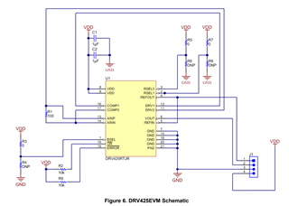
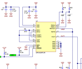
What is the difference between the schematics from Figure 1 DRV425EVM and Figure 2 from TIDA 00463.
In figure 1, The shunt resistor is on the trace bewteen DRV2 (Pin 11) and COMP2 (Pin 17)
In figure 2, The shunt resistor is on the trace bewteen DRV1 (Pin 12) and COMP1 (Pin 16)
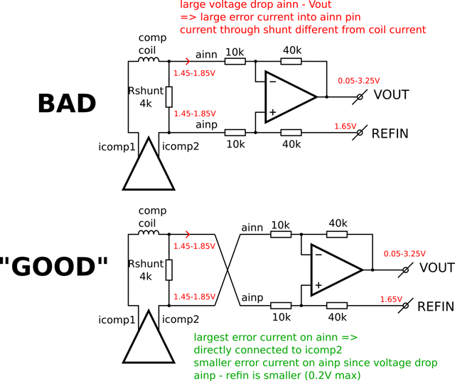
How does it impact the design? Is there a specific reason for this config? Does it affect the measurement or sensitivity?

Figure 1 - DRV425EVM

Figure 2


