This thread has been locked.

If you have a related question, please click the "Ask a related question" button in the top right corner. The newly created question will be automatically linked to this question.

IWR1843BOOST: IWR1843BOOST

Part Number: IWR1843BOOST
Other Parts Discussed in Thread: UNIFLASH, IWR1843

Tool/software:

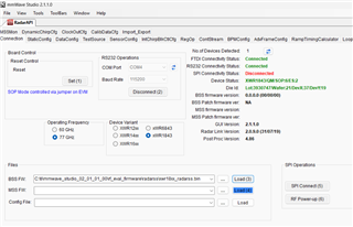
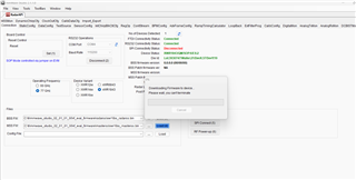
I am attempting to get an IWR1843BOOST with an ADC1000 up and running with mmWave Studio 2.1.1.0.  I have successfully loaded the demo BSS firmware as shown in the first screenshot.  However, when attempting to load the MSS firmware the system appears to lockup, as shown in the second screenshot.  One oddity that I noticed is that the BSS firmware is shown as 0.0.0.0 with a date of 00/00/00.  The BSS file loads reasonably quick.  The MSS stays stuck on 0% loaded for more than five minutes.  I have tried this twice now with the same results. Thoughts on how to troubleshoot this?

  • Hello,

    Please check the DCA1000 E2E FAQ post for all information relating to the DCA1000. My guess is that the hardware switches/SOP modes may be incorrect for DCA1000 mode.

    https://e2e.ti.com/support/sensors-group/sensors/f/sensors-forum/1441304/faq-dca1000evm-support-tools-debugging-and-more

    Best Regards,

    Pedrhom

  • Here are the switch settings I have...

    IWR1843BOOST...

    SOP mode (debug/development mode).
    SOP0: Off
    SOP1: On
    SOP2: On

    S2:  SPI

    On the ADC1000...

    LVDS_MODE_SEL: 

    16BIT_ON
    14BIT_OFF
    12BIT_OFF

    SW2...

    LVDS_CAPT:  OFF
    SD_STORE:   OFF
    1243_MODE:  OFF
    RAW_MODE:  OFF
    HW_CONFIG: ON
    USER_SW1: OFF
    USER_SW2: OFF
    USER_SW3: OFF

    Note: I did flash "mmwave_sdk_03_06_02_00-LTS\packages\ti\utils\ccsdebug\xwr18xx_ccsdebug.bin" which is something I believe is needed to utilize debug/development mode in order to load the rf_eval_firmware bss and mss files.  Should I be flashing something different?


  • Hello,

    rf_eval_firmware bss and mss files would overwrite any .bin flashed to it prior. So although not used, having flashed xwr18xx_ccsdebug.bin should not have affected anything in theory. That said please check the photos for switches in this user guide. They are wrong based on what you have written

    https://dev.ti.com/tirex/explore/node?a=1AslXXD__2.20.00.05&node=A__AGTrhNYW8jE6cMxbovlfaA__radar_toolbox__1AslXXD__2.20.00.05

    Best Regards,

    Pedrhom

  • Per the DCA1000 mmWave Studio User Guide:  "Make sure your device’s SOP mode is in “Development” mode, which is where SOP0 and SOP1 are ON and SOP2 is OFF with regards to the mmWave sensor."  However, whenever I configure for this mode the NERR light illuminates (see "Debug Fails" picture) and I am not able to connect to the device via CCS.

    .

    When I configure as follows: SOP0: OFF, SOP1: ON, SOP2: ON, the NERR light is off (see "Debug Good" picture) and I am able to connect via CCS and load and step through an application.


    I have seen this behavior even before adding the DCA1000 module to the 1843 EVM.

    Thank you,

    Ron 

  • Hello Ron,

    Why are you trying to connect to the device via CCS when in Development/DCA1000 mode? When the radar sensor is set like this, the DCA1000 interfacing is what will be working. Ignoring the LED, are you able to connect in mmWaveStudio like this?

    Best Regards,

    Pedrhom

  • I am not trying to connect to the device via CCS when attempting to use the mmWaveStudio.  I am just trying to point out that there might be an issue with how the dip switch settings are documented.  The mmWaveStudio and CCS both seem to want development mode (which I assume is the same as debug mode) to have SP2: Off, SP1: On, SP0: On.  However, I have not been able to get debug to work with CCS with those dip switch settings.  The only way that I can get CCS to work with this device is with the dip switch settings SP2: On, SP1: On, SP0.  Wonder if this is an issue with Rev C of the board (which has dipswitches instead of jumpers)?

  • Noticed a typo in my message above. The second to the last sentence should read: The only way that I can get CCS to work with this device is with the dip switch settings SP2: On, SP1: On, SP0: Off.

  • Hello,

    This makes sense, and I see where the problem is. The naming terminology here is definitely confusing since we are using "debug" twice but meaning two different things. CCS only needs the device in either functional or flashing mode to run CCS Debug for application code debug. Debug hardware configuration mode is for raw data capture and other front-end RF, chip level debug, aka DCA1000 + mmWaveStudio.

    Best Regards,

    Pedrhom

  • Hi Pedrhom,
    Thank you for the feedback. I am getting a clearly picture now of how this works.
    A related question to further clarity... 
    For flashing the onboard QPSI device with the CCSDebug.bin, I expect the XDS110 emulator uses just the JTAG interface for that.  Then when the device is rebooted in functional mode, would it be correct that the CSSDebug.bin application communicates with CCS over the UART, not JTAG?   Or does CSS continue to use both the UART and JTAG for debug operations?  Or is the UART just for the initial download?

    Thank you again,

    Ron

  • Hello Ron,

    When you are flashing using Uniflash or any similar tool to flash a .bin, you boot over UART and that is how the binary is flashed. When you have a .out, and load it in CCS for debug, you are loading the memory via JTAG. You have to be in flashing mode to flash .bin over UART, whether this be application code or the CCSDebug image that allows JTAG (C:\ti\mmwave_sdk_03_06_00_00-LTS\packages\ti\utils\ccsdebug\xwr18xx_ccsdebug.bin). Afterwards in functional mode, you either automatically run your application if you flashed a demo or manually load in the .out over JTAG to run if you flashed CCSDebug.

    Best Regards,

    Pedrhom

  • So, if I load my application via CCSDebug (which uses JTAG), then my application is free to use the UART when it starts running?

  • That is correct, once running after the firmware is loaded via one of the two methods, communicating with the device during run time is the same. The bonus of flashing .out over JTAG using CCS allows the use of the XDS Debugger to place break points and browse memory during pauses. As well as not having to constantly set the device mode back and forth between flashing and functional.

    Best Regards,

    Pedrhom

  • One thing I am still confused about is regarding this statement: "When you are flashing using Uniflash or any similar tool to flash a .bin, you boot over UART and that is how the binary is flashed".  I would think that for the target device to utilize the UART, it would already need an executable running.  This seems to be a chicken-and-egg problem.  If we have a corrupted flash, how would Uniflash communicated with the device?  My sense is that Uniflash would only use JTAG for programming the flash device, not the UART?

  • Perhaps we might need to clarify.  My understanding is that the XDS110 emulator instantiates two serial interfaces via the USB connection: 

    • "Class Application/User UART"
    • "Class Auxiliary Data Port"

    Are these just pass through to IWR1843 device?

  • Hello Ron,

    Let me be more clear as what you said is true but was not what I meant to portray: the image is accepted over UART, and loads it to the serial flash connected to the QSPI port. If there is a corrupted flash, you are able to erase the SFLASH in Uniflash on the "Settings & Utilities" tab.

    For more details on flashing mode and what exactly happens and how, check the Technical Reference Manual for generation 1 mmWave device. https://www.ti.com/lit/pdf/swru522

    Best Regards,

    Pedrhom

  • Thanks, Pedrhom, the pieces are starting to come together...

    I assuming you are referencing section "4.5 Boot" of the IWR Family TRM? Ok, starting to understand better, I think. But still unclear on some things. The background here is that our production board is going to be very tight on real-estate, so we are not going to be able to have the standard headers for connecting a real XDS110 debug probe. Our hardware guys are thinking we should be able to program the flash device and debug the application solely using the JTAG interface. However, it sounds like Uniflash must have the Application UART connected to program the flash? (To confirm, the boot ROM is actually flashing the device. Uniflash is just communicating with the boot ROM via the UART interface. Correct?)

    Related, I see inconsistencies in documentation that is confusing. Section 4.5 of the IWR Family TRM indicates there are only two SOP configurations that are of use and that the others "result in unknown device behavior". However, the xWRI1843BOOST Users Guide indicates three SOP configurations. And even further, the xWRI1843BOOST schematic indicates five SOP configurations. Possibly to clarify what is what regarding use of the three SOP switches?

    What is the CCSDebug.bin doing that the boot ROM is not doing? Why sense is that the boot ROM is used for simple boot and flashing support, whereas CCSDebug additionally initializes the various subsystems into a usable state. CCSDebug then also provides support for downloading MSS and DSS applications to RAM and launching them? And once the applications are launched, the UARTS are no longer used for booting / debugging? After that, all debugging takes place via JTAG?

    If all of that is making sense, then in a target system where the applications is booted via flash, I can still debug via JTAG (without further need for the UART)?  However, I cannot flash the QSPI device via JTAG alone?

  • Hey Ron,

    For more context on the ccsdebug.bin image and what it does, please see "CCS development mode" within "Loading images onto mmWave EVM" of the SDK 3.6 User Guide (page 8-9)

    https://dr-download.ti.com/software-development/software-development-kit-sdk/MD-PIrUeCYr3X/03.06.00.00-LTS/mmwave_sdk_user_guide.pdf

    For 1843BOOST EVM, you can ignore SOP configurations outside of flashing and functional modes, and debug mode is only if you are interested in raw data and only works in tandem with a DCA1000. The last two that are seen in the schematic are unused and don't do anything, hence it resulting in "unknown device behavior". What is shown in the 1843BOOST EVM User guide (Section 2.8.1 page 13) is what is most up to date and specific to that EVM, while the TRM is for chip level information. This results in the occasional discord between TRM and EVM User Guide/design since the TRM/chip comes first. Especially when we have revisions to EVMs.

    https://www.ti.com/lit/spruim4

    Once a demo application is launched, and a valid configuration is either hardcoded or sent over CLI, the UART configuration port is no longer needed, and the UART data port is used to get the output data. This will be the case regardless of how application code is loaded to the device. There are other possible ways of getting output data such as SPI/CAN/I2C, but that will require custom changes integrating those drivers (also in the SDK) into the demo. By default we use UART and is how all of our example demos work due to simplicity.

    After a one time flashing of the CCSDebug.bin over UART, you can flash the QSPI device via JTAG alone as many times as you'd like.

    Best Regards,

    Pedrhom

  • Hi Pedrhom,

    Thank you for the clarification of the dip-switching settings.  All good there now.

    I am confused by "After a one time flashing of the CCSDebug.bin over UART, you can flash the QSPI device via JTAG alone as many times as you'd like.".  I would think that if I flashed the QSPI device via JTAG alone, then that would have replaced the CSSDebug.bin with whatever I had replaced it with.  This seems to indicate that CCSDebug is not needed to use JTAG alone? 

    Also, I haven't found anything solid as to how to use Uniflash (version 9.1) or CCS (version 20.1) with JTAG only.  Uniflash seems to require a COM port.  For CCS, the mmwave sdk user's guide states "Debug/JTAG capability is available via the same XDS110 micro-USB port/cable on the EVM. TI Code composer studio would be required for accessing the debug capability of the device. Refer to the release notes for TI code composer studio and emulation pack version that would be needed.", but I haven't been able to figure that out.

    Thank you again... making progress here. I very much appreciate your patience with this newbie to these devices and tools.

    Ron


  • Hey Ron,

    We have a JTAG Flasher tool that allows the flashing of a MetaImage .bin via JTAG without any UART interface. The user guide is on the Radar Toolbox in the TI Developer Zone.

    https://dev.ti.com/tirex/explore/node?node=A__AWIoiRGl9nAtaaUSJLDghw__radar_toolbox__1AslXXD__LATEST

    Best Regards,

    Pedrhom

  • To confirm, I can use the JTAG Flasher tool WITHOUT having to have first flashed CCSDebug.bin, correct?  And this tool will work with the XDS110 (whether simulated on EVM or using a real XDS110)?

  • You can use the JTAG Flasher tool without the CCSDebug.bin image. And this tool is meant to be used with the XDS110 since it is what is used with our EVMs. Section 5 of that JTAG Flasher user guide briefly covers what needs to be done to have it work with other IDE or other JTAG emulators.

    Best Regards,

    Pedrhom