This thread has been locked.

If you have a related question, please click the "Ask a related question" button in the top right corner. The newly created question will be automatically linked to this question.

IWR6843AOP: bare minimum / recommended PCB stack up

Part Number: IWR6843AOP

Tool/software:

Hello Experts,

i was building pcb design and wanted to know the bare-minimum requirements for PCB.

I don't even need traces like LVDS i only need UART connection ( of course pcb will be as per swr166 / sprr418 - required parts only  )

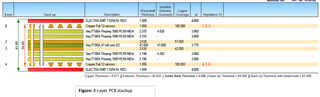
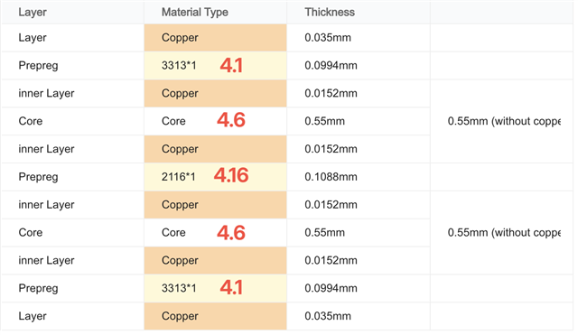
i have read pcb stacks that were available on xWR6843AOP_HW_BringUp_Schematic_and_Layout_Checklist.

General information on the documents and forum is to use recommended stackup to avoid performance degradation.

however, i read that whole point of AOP is relaxed pcb requirements as antennas are on package.

i was wondering what is minimum i can get away with for prototyping / initial small manufacturing WITHOUT ANY performance degradation.

Please bare with me as i am quite new to this.


Is any of below sufficient for stripped down version of reference design ?


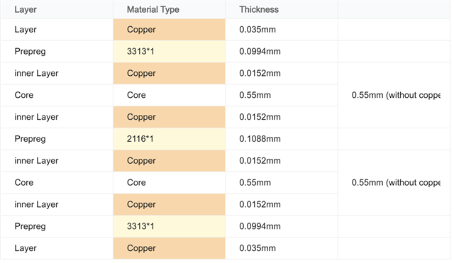
Thank you in advance for your help.

  • Hi

    Thanks for your query. Please allow us a couple of days to respond

    Regards

  • Hi there,

    If you want to reduce the overall PCB cost, you can go for four-layer PCB. Could you please let me know how many layers do you require?

    For a 4-layer PCB you can refer to the below stack-up:

    Also, the stack-up you have shared, could you please specify the dielectric type and more information about it?

    Also, please let me know what all communication interfaces you would require. 

    Thanks,

    Swarnendu

  • Hello Swarnendu,

    Thank you for your response.

    Dielectric type is FR4.

    Surface Finish: ENIG

    Thickness: 1.6mm

    Outer Copper Weight: 1oz

    Inner Copper Weight: 0.5oz

    Please find updated image i have written dielectric constant ( In red colour).


    "North and South side of the PCB should be as close as possible to the device to reduce the surface wave effects. East and West side of the PCB should have a minimum spacing of one lambda (~5mm) from the device to PCB edge or any other components."

    After reading your answer here. i am trying to make it as compact as possible that is why i choose 6 layer ( 4 layer works for me). i am aware of trapezoid cutout solution and please correct me if i am wrong but i am assuming that having compact pcb will still have better performance.

    i am building modular system (b2b connectors on the bottom-side ) and current communication requirement is UART and couple of GPIO. (USB_TO_UART - CP2105 is not part of PCB ).
    After reading this i am considering SPI as well.

    Please let me know if anymore information is required.

    Thank you

  • Hi,

    I have reviewed the dielectric constants, this looks fine.

    FR4 material is okay.

    ENIG surface finish is also fine as the antenna is on the package itself.

    Overall PCB thickness of 1.6mm is okay.

    The copper weight is also okay.

    Yes, that is correct, the surface wave artifacts need to be considered for designing the PCB.

    I hope you have already referred to the device errata in this regard:

    https://www.ti.com/lit/er/swrz092b/swrz092b.pdf? (PACKAGE#02 Surface Wave Artifact from PCB)

    You can make the PCB compact, however, I would recommend placing all the components on the other side of the PCB of which the device resides. If it is absolutely necessary to place some components on the device side of the PCB, please maintain at least one wavelength (~5mm) on the East and West side of the PCB. Please keep the North and south sides of the PCB edges as close as possible to the device edges.

    For SPI/UART communication interfaces, the stack up looks okay. 

    Please also consider care abouts of thermal design aspects. Please refer to the application note:

    Thermal Design Guide for Antenna on Package mmWave Sensor 

    Thanks,

    Swarnendu

  • Hello,

    All the components are planned to go on the other side of the PCB. however, 40mhz crystal oscillator was planned on the side of device ( trying to avoid vias). do you recommend putting that on the other side as well ?

    Thank you.

  • Hi Maharshi,

    That is okay. Please consider the guidelines for component placement on the Device side.

    Thanks,

    Swarendu

  • I had shared 2 stackups with you. both of them are okay to use ?

    do you recommend one over other ?

    I am marking this as resolved.

    Thank you so much for you help.

  • Maharshi,

    Both of the stack-ups that you shared are okay for RF and relevant performance for the IWR6843AOP.

    Thanks! Glad to help you.

    Best regards,

    Swarnendu