This thread has been locked.

If you have a related question, please click the "Ask a related question" button in the top right corner. The newly created question will be automatically linked to this question.

AWRL1432: Regarding the issue of downloading firmware via uniflash

Part Number: AWRL1432
Other Parts Discussed in Thread: UNIFLASH, , , CCSTUDIO, LP-XDS110, LP-XDS110ET, IWRL6432BOOST

Tool/software:

Hello, expert

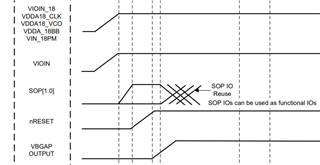
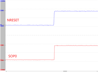
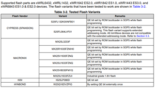
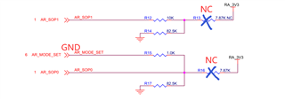
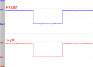
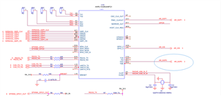
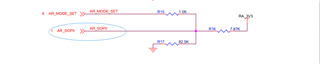
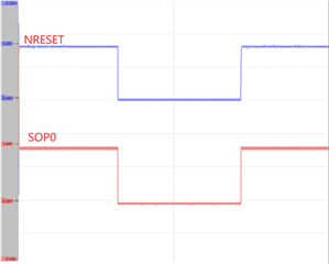
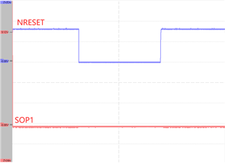
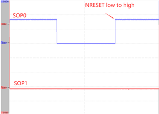
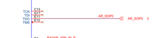
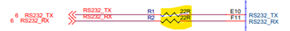
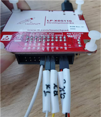
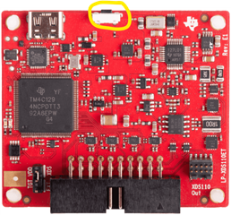
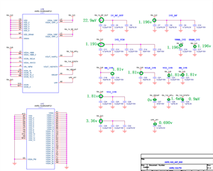
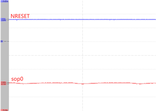
        this is waveform for SOP0 and NRESET at the time of reset release.(P1, my chip is l1432)

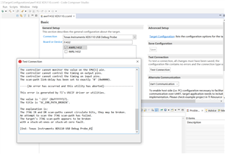
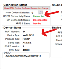
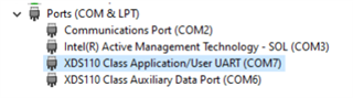
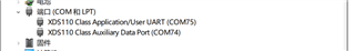
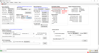
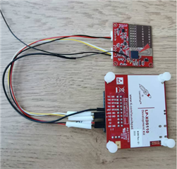
        When I was flashing the device using uniflash, the flashing program would get stuck at "send break signal".

        Just as described here https://e2e.ti.com/support/sensors-group/sensors/f/sensors-forum/1502524/iwrl6432-about-the-l6432-flash-problem


           Are there any other suggestions?


Thanks.

  • Hi Tony,

    Thank you for reaching out. Please allow us a few days to investigate this issue.

    Best,

    Vignesh K.

  • Hi Tony,

    Thanks.

  • Hi Tony,

    The above plot you have shared for SOP and nReset does not describe whether SOP signals are stable before the nReset is released. Can you also share the plot of SOP and nReset similar to the below image?


  • Hi, 

    The following picture is about the circuit diagram of the flash part. I changed the U2 position to W25Q16JVUXIQ\MX25R1635FZUIL0\MX25R1635FZUIL0, but I still got an error when flashing. (The flash model and package in the sprach9g.pdf table that can be fully matched are MX25U1633FZUI, but this one is incompatible with the 1.8v voltage and the 3.3v of the circuit board, Among the other three tests, only the final letters are not allowed
    )


    The following is the variation waveform of sop0 of Nreset from low level to high level. I added a button at both ends of c1. The low-level part of nreset is the waveform when the button is pressed. The flashing starts 3 to 5 seconds after the waveform changes from low to high.


    Thanks.

  • The last picture is an enlarged view of the rising edge part

  • Hi Tony,

    Appreciate your patience here. The AWRL1432 device does not support the flash variants:MX25R1635FZUIL0\MX25R1635FZUIL0 because of its low frequency support in quad mode (<80MHz). The W25Q16JVUXIQ has not been tested by us. Please use any of the flash variants mentioned in the below list which are tested for AWRL1432 device.

    Thanks,
    Deexith.

  • Additionally, we recommend placing termination resistance of 33.2ohms for all QSPI high speed lines to avoid reflections. These terminations resistors play a key role if the QSPI flash part is placed far from the AWRL1432 device.

    Thanks.

  • Hi Deexith,

    We tested the IS25LP080D in the table, but the flashing problem still exists.

    The distance of the spi line from our flash to l1432 is about 1.5cm.

    There is one thing I'm not sure about here. Are the waveforms of NRESET and SOP0 I sent above normal after resetting?

    Are there any other possibilities that might cause our problems?

    Thanks,

    Tony.

  • Hi Tony,
         Can you please confirm which SOP mode the device is kept when you are trying to flash it? For flashing the device, it should be kept in Device Management Mode/ QSPI Flashing Mode where SOP0 = 0, SOP 1 = 0.


    Thanks and Regards,
    Sivaprasad

  • Hi Sivaprasad,

          As shown in the following figure, both of these two points are at a low level in the external circuit.


    Thanks.

  • Hi Tony,
    From the waveform you have shared, it looks like SOP0 is dependent on nReset signal.

    SOP0 is transitioning to low/high level w.r.t nReset signal level. Can you please let me know the reason for that? Can you please also let me know where this AR_MODE_SET signal is connected to? Please try flashing the device after removing R15. As I mentioned before, SOP0 & SOP1 supply should be 0v and stable before nReset release for the device to boot up in QSPI Flashing Mode.

    Thanks and Regards,
    Sivaprasad

  • Hi Sivaprasad,

    As shown in the picture, the other end of the AR MODE SET is connected to GND.

    According to your suggestion, I attempted to remove R15 and examine the waveform of sop0. It is highly correlated with NRESET. When NRESET changes from low level to high level, SOP0 changes simultaneously (just like the waveform diagram I sent above).

    After removing R15, SOP0 was only connected to GND through R17, and that high-level signal seemed to be emitted by L1432.

    Thanks.

  • Hi, 

    I also tried the MX25V1635FZNQ03 chip of the same type as the AWRL1432BOOST-BSD development board through a flying cable, but it still reported an error.

    The following picture is a screenshot of the pcb of our board. Please also help check if there are any errors.

    Thanks.

  • Hi Tony,
         SOP0 is a input pin of AWRL1432 and it will not emit anything out. Looks like SOP0 is pulled up and AWRL1432 is powered up in functional mode
    (SOP0 :1, SOP1 : 0) instead of QSPI flashing mode (SOP0 :0, SOP1 : 0). Flashing the device(with Uniflash) will fail if the device is not powered up in QSPI flashing mode. Can you please share complete schematic associated with AR_SOP0 signal? I would like to check if AR_SOP0 is connected to nReset or 3.3V at any point. Can you please also capture SOP1 signal along with nReset & SOP0?

    Thanks and Regards,
    Sivaprasad

  •  Hi Sivaprasad,

    I have requested cayden to send you all the pdf schematic diagrams via ti's email.

    I also checked the schematic diagram at the same time. As shown in the following figure, AR_SOP0 has connections only at two positions marked with blue circles, and not at others points.


    My oscilloscope has only two inputs and it is impossible to obtain the waveform diagrams of three points simultaneously.

    The following are the waveform diagrams obtained in three installments

    Thanks.

  • Hi Tony,
         Thank you for the information. Can you please double check in the PCB whether R16 is populated or not? Can you please read the location "0x5B020008" through CCStudio by powering up the device in QSPI Flashing mode? It will give the information on SOP configuration with the device is actually powered up. Therefore, it will help to confirm our suspicion and isolate the failure to incorrect SOP configuration. 

    Thanks and Regards,
    Sivaprasad

  • Hi Sivaprasad,

    R16(and R15) on the pcb has been removed,
    Since there are no xds110 and l1432 connections on our board, I directly connected RS232_TX(E10) and RS232_RX(F11) to the computer via cp2102.
    I'm not sure whether this hardware connection method can be supported by ccs?
    I attempted to connect the device using the "Data Snapshot Viewer" method in "Target Configurations", as shown in the following figure. It seems that I couldn't connect the device.
    Or is it possible to read the information of the location "0x5B020008" by other methods? Could you give me a schematic diagram?
    Thanks.
  • Hi Tony,
         JTAG connection is required for reading register through CCStudio. Apologies for the request. There is no other way to read this register in QSPI flashing mode/Functional mode. Can you please share zoomed in scope shot of rising edge of SOP 0 w.r.t rising edge of NReset?

    Thanks and Regards,
    Sivaprasad

  • Hi Sivaprasad,

        This is the waveform after the rising edge is well-developed


    Thanks.

  • Hi Tony,
         Thank you for sharing the scope shot. Can you please mark X-axis with the "time" for better understanding and share more zoomed in scope shot of rising edge if possible. Please also add a vertical curser at 0.96V of nReset.

    • Can you please share complete schematic of the design?
    • Can you please try flashing with the XDS- Launchpad (LP-XDS110ET/ LP-XDS110)? 
    • Is this issue seen across multiple PCBs?

    Thanks and Regards,
    Sivaprasad

  • Hi Sivaprasad,

        I'm sorry that the exported picture has no time information. The following one was taken directly by me (hope it's useful).

        Each cell on the vertical coordinate is 1v, and each cell on the horizontal coordinate is 10ms. The cursor T has moved to around 0.96v.

        CH1 (yellow) is NRESET and CH2 (blue) is SOP0.


        The following file is the complete schematic diagram

        AWRL1432_BSD.pdf

        The points such as TCK, TDI and TMS of our board are not led out from the chip, so I may not be able to connect to the board using xds110.


        I have a total of three development boards, and none of them can flash the firmware.


    Thanks  


  • Hi Tony,

    • Thank you for sharing the zoomed in scopes shot and schematic files. I am reviewing it.
    • You don’t need JTAG connectivity for using XDS Launchpad. You can connect RS232 and GND pins to XDS-LP and use it for flashing the AWRL1432 device. Can you please try flashing with the XDS- Launchpad (LP-XDS110ET/ LP-XDS110)?
      LP-XDS110ET Evaluation board | TI.com, LP-XDS110 Development kit | TI.com
    • RS232/UART connectivity check with the current setup
      • Put the device in debug mode (SOP0 : 1 , SOP1 : 1)
      • Connect to COM port in mmWave studio
      • There is an option in RFEval tab mmWaveStudio to read registers.
        For example you can try reading “0x5B020008”
    • Power Up sequence and hardware connectivity check
      • Power up the AWRL1432 PCB first
      • Connect RS232 pins of AWRL1432 to UARTtoUSB converter. Please note, RS232TX pin should be connected to RX pin of UARTtoUSB converter and RS232RX pin should be connected to TX pin of UARTtoUSB converter. There should be a common GND connection between AWRL1432 PCB and UARTtoUSB  converter PCB.
      • Power up the UART to USB converter PCB

    Thanks and Regards,
    Sivaprasad

  • Hi Sivaprasad,

    Thank you for your detailed instructions. I won't be at the company this week and will return in the first week of June.

    I will conduct the test immediately then. I referred to this(https://www.ti.com/lit/zip/sprr479(LP-XDS110: Schematic)) schematic diagram file.


    Please help check if my understanding of the wiring is correct (as shown in the picture below),I'm surprised that there are only these signal lines?


    Thanks.

  • Hi Tony,
         Yes, your understanding about the connection is correct. You can also connect XDS_RESET_LS to NRST signal and issue reset from LP-XDS110.
    Please note, Power Up sequence and hardware connectivity check that I mentioned in the previous section is also applicable for whatever the UARTtoUSB connector that you are using.

    Thanks and regards,
    Sivaprasad

  • Hi Sivaprasad

    The version of XDS that I am using is "LP-XDS110".

    I connected the hardware circuit as you described in your previous post, and set the SOP to 11.

    I have newly created a "Target Configuration". When I clicked on "test connection", I received the following error.


    The detailed error log is as follows

    [Start: Texas Instruments XDS110 USB Debug Probe_0]
    
    Execute the command:
    
    %ccs_base%/common/uscif/dbgjtag -f %boarddatafile% -rv -o -S integrity
    
    [Result]
    
    
    -----[Print the board config pathname(s)]------------------------------------
    
    C:\Users\lux\AppData\Local\TEXASI~1\CCS\
        ccs1271\0\0\BrdDat\testBoard.dat
    
    -----[Print the reset-command software log-file]-----------------------------
    
    This utility has selected a 100/110/510 class product.
    This utility will load the adapter 'jioxds110.dll'.
    The library build date was 'Apr 19 2024'.
    The library build time was '14:04:01'.
    The library package version is '12.7.0.00130'.
    The library component version is '35.35.0.0'.
    The controller does not use a programmable FPGA.
    The controller has a version number of '5' (0x00000005).
    The controller has an insertion length of '0' (0x00000000).
    This utility will attempt to reset the controller.
    This utility has successfully reset the controller.
    
    -----[Print the reset-command hardware log-file]-----------------------------
    
    The scan-path will be reset by toggling the JTAG TRST signal.
    The controller is the XDS110 with USB interface.
    The link from controller to target is direct (without cable).
    The software is configured for XDS110 features.
    The controller cannot monitor the value on the EMU[0] pin.
    The controller cannot monitor the value on the EMU[1] pin.
    The controller cannot control the timing on output pins.
    The controller cannot control the timing on input pins.
    The scan-path link-delay has been set to exactly '0' (0x0000).
    
    -----[An error has occurred and this utility has aborted]--------------------
    
    This error is generated by TI's USCIF driver or utilities.
    
    The value is '-233' (0xffffff17).
    The title is 'SC_ERR_PATH_BROKEN'.
    
    The explanation is:
    The JTAG IR and DR scan-paths cannot circulate bits, they may be broken.
    An attempt to scan the JTAG scan-path has failed.
    The target's JTAG scan-path appears to be broken
    with a stuck-at-ones or stuck-at-zero fault.
    
    [End: Texas Instruments XDS110 USB Debug Probe_0]
    

    When I ignored this test and forcibly started the target, the target indicated that it couldn't be linked.

    I didn't figure out that I made a mistake at that step, which caused me to be unable to connect to the device.

    Thanks.

  • Hi Tony,
         I was referring to mmWaveStudio which you can download from the following link AWRL1432 data sheet, product information and support | TI.com under software development section.

    • Put the device in debug mode (SOP0 : 1 , SOP1 : 1)
    • Connect to RS232 comp port in mmWaveStudio


    • There is an option in RFEval tab mmWaveStudio to read registers.
      For example you can try reading “0x5B020008


    Thanks and Regards,
    Sivaprasad

  • Hi Sivaprasad,

    Thank you for sending the detailed information.

    I checked the hardware connection status of 5V, GND, RX, TX and nRST, and also checked the level of SOP (which was 11).

    As shown in the two figures below, after I opened mmWaveStudio and selected the serial port, and clicked the connection button, the status on the right side would never show that the connection was successful. If I ignored this error, when I moved to the RFEval page and checked the value of the "0x5B020008" register, it showed 0.

    When I used the iwrl6432boost development board to test the mmWaveStudio tool, I could see that the green light in the connection status area was on, and I was able to read that the value of the 0x5B020008 register was 0x03.The following picture is a screenshot of the development board.

    IWRL6432BOOST read

    Thanks.

  • I'm sorry, but there might be an issue with the uploaded images. The last one should be deleted as it is the same as the first one (I should have deleted it).

  • Hi Tony,
         Once RS232 COM ports connect successfully, you will be able to see RS232 connectivity status and device status getting updated in mmWaveStudio as you have seen with the Boost EVM. 


    0x5B020008 register should read 0x03 for debug mode (SOP0 : 1, SOP1 : 1).

    • Can you please share a picture of the setup and mark the connections?
    • Can you please confirm whether you are connecting to Application/User UART COM Port or not?

    • Can you please confirm whether a jumper is placed on the 1-2 pin of the P9 connector of the LP-XDS110 (yellow circle in below snapshot)

    • Are you following the powering sequence as mentioned below?
      • Power up the AWRL1432 PCB first
      • Connect RS232 pins of AWRL1432 to UARTtoUSB converter. Please note, RS232TX pin should be connected to RX pin of UARTtoUSB converter and RS232RX pin should be connected to TX pin of UARTtoUSB converter. There should be a common GND connection between AWRL1432 PCB and UARTtoUSB  converter PCB.
      • Power up the UART to USB converter PCB
    • What is the reason for keeping 22 ohm resistor in RS232 lines? Can you please short it?


      Thanks and Regards,
      Sivaprasad
  • Hi Sivaprasad,

    I operated according to the following steps.

    step1. Weld a 1k resistor onto R13 and R16. After powering on, measure that both AR_SOP1 and AR_SOP0 are 3.3V. Remove R15 and leave AR_MODE_SET open.

    step2. The power port of the equipment is first connected to the XDS. The nRST black wire is soldered to R5, near the NRESET end. The other black wire of the button is soldered to the ground, and the button is in the off state.


    step3. The USB end of xds is connected to the computer.

    step4. Open mmwaveStudio and connect the serial port.hen observe that the RS232 status remained disconnected. (In the step3, I have tried both the serial port 74 and 75 that I saw.)

    This is the complete set of my operation steps.

    LP-XDS110 P9 My line is consistent with the picture you sent.

    When I short-circuited the wires of R3 and R4, I still couldn't connect to the device. (The resistance on the line is to consume the energy of the reflected signal wave.)

    Thanks.

  • Hi Tony,
        Thank you for the detailed explanation. RS232 COM port connectivity is just a basic check. Now I am suspecting whether the device is working and/or supplies are fine or not. Can you please share scope shot of all the internal/external power supplies with it's level marked?

    Can you please power up the device in functional mode (SOP0 : 1, SOP1 :0) and measure across any de-coupling capacitor of 3.3V , 1.2V Dig/RF/SRAM, 1.8V, VBGAP, 1V RF, APLL and SYNTH rails? 

    Can you please also remove "key" from the nRST wire connection? You just need to connect nRST signal of LP-XDS110 to nRST signal of AWRL1432 PCB (R5, near the NRESET end). You can issue nReset from LP-XDS110 by pressing the switch (circled in yellow). As you are powering the AWRL1432 PCB from LP-XDS110, you should issue an nRST from LP-XDS110 after the power up.


    Thanks and Regards,
    Sivaprasad

  • Hi Sivaprasad,

    After handling that additional case, The end of the AR_MODE_SET wire is still hanging loose, and the R15 resistor has not been soldered., I proceeded to measure the voltage value after pressing the "nRST button" on the LP-XDS110.

    The voltage value is indicated in green as shown in the following figure.In addition, the input provided by LP-XDS110 is 4.99V. (device in functional mod SOP0 : 1(3.35v), SOP1 :0(2.7mV))

    Thanks.

  • Hi Tony,
          Thank you for performing voltage measurements. If you see all the internal supplies are 0V (VBGAP, 1v4_Synth, 1v4_APLL,1V_RF) which indicates that AWRL1432 IC is damaged.


    Thanks and Regards,
    Sivaprasad