Because of the Thanksgiving holiday in the U.S., TI E2E™ design support forum responses may be delayed from November 25 through December 2. Thank you for your patience.

This thread has been locked.

If you have a related question, please click the "Ask a related question" button in the top right corner. The newly created question will be automatically linked to this question.

OPT8241&OPT9221:Laser diode drive circuit

Other Parts Discussed in Thread: OPT8241, OPT9221, TPS2559

Dear all,
I have downloaded the "OPT8241-CDK-EVM Hardware" ,but I can't understand the part of Laser diode drive circuit fully,especially the "Illumination Path Delay Correction Using Feedback".
Please let me know if my following understanding is correct or not.
The drive ckt is similar to a boost DC-DC ckt,the difference is that there are none caps at the point after the inductor,then the diodes off when the MOS U15 on,while it on when U15 off.The duty cycle of TRIG_G is 50%,but the laser diodes on is difficult to reach 50% because of the existence of Switch Delay Time of the MOSFET.The ZENER diode and BAP65-02 diode limit the max drive voltage at about 10V(5+3.9+0.9),It works in constant voltage driving mode?Or it works in variable current driving mode usually,while the voltage is limited to avoid damaging the laser diode?

Otherwise I have the following questions:
1// Why use "C52" here? Is there any connection between the cathode of D16 and the vRef ?
2// "OPT8241 Evaluation Module User Guide.pdf" mentioned "The illumination power can be changed only between 40% to 100% of the total power".Why the power can be controlled by changing the vRef voltage? How it works?Why it is "40% to 100%".
3// Can you provide me with any more details about "Illumination Path Delay Correction Using Feedback"?for example,the signal wave of "COMP_MOD_REF","COMP_MOD_FB"...what's the duty cycle...help me to understand.
4// I can't find the datasheet of the laser diode,can you provide me?

My email is chenqianzuan@uniview.com.

thank you!

  • Dear Zuan,

    Thank you for showing interest in the product. Your understanding of the laser diode switching circuit is very accurate. The combination of Zener diode and BAP65-02 works as a very fast acting snubber circuit which takes away all the ringing energy from the circuit by clamping the voltage. It also helps in freewheeling the inductor. The third and the final function of the Zener diode + BAP65-02 combination is that it protects the MOSFET against voltage surges.
    I will get back to you on your 4 questions in a day.

    Regards,
    Subhash
  • Hi Subhash,
    Thank you for your reply.
    How are things going?

    Regards,
    Zuan
  • Zuan,

    I will first explain the general functioning of the illumination delay path correction. This circuit is meant to measure the delay of the illumination circuit. We try to measure the delay from Illum_P / Illum_N signal to the light coming out from the laser and it is then subtracted in the TFC(OPT9221, Time of Flight Controller) from every pixel in each frame.

    How we implement it is that we have a comparator monitoring the current through the laser diode. The moment laser diode current increases beyond a certain value, the comparator output changes state. This digital output is then fed to the TFC which measures it against Illum_P/Illum_N. If we just leave it at that, TFC would not be able to account for the propagation delay of the comparator. So we have another comparator in the same package and TFC measures the loop delay through that comparator using the COMP_MOD_REF signal. The XOR gate tells you the difference in delays which is measured by the TFC.

    Answers to your question:

    1. The comparator is supposed to sense the current through D16. We approximate the model of the diode as a resistor and also account for the parasitic inductances. The RC network compensates for the effect of the inductance and the comparator sees only the effect of the current rise through the diode. However, we also expect the cathode of D16 to have significant ground bounce. So it is important to AC couple D16 cathode with the vRef. C52 helps in that AC coupling.

    2. vRef, helps in deciding the "trip level" of the comparator. It is only for the delay feedback compensation. We are limited to a minimum of 40% optical power because of the limitation of the current source IC, TPS2559. This IC takes a voltage input and acts as a current source which we use to drive the lasers.

    3. I have explained this above.

    4. Laser datasheet is attached.8357.22045498_Rev003 Datasheet.pdf

    Hope this answers your questions.

    Regards,
    Subhash

    http://www.ti.com/lsds/ti/sensors/3d-imaging-sensors-overview.page#design

  • Dear Subhash, 
    Thank you for your answers. 
    I've just seen the "RVar" net here,I kown how to change the power now. 
    vRef decides the "trip level" of the comparator,it means that there may be a rather non-ignorable error in the delay measurement from Illum_P to the light especially when the edge is not very steep? 
    I guess I understand how it works roughly before(accord with your explanation),and I kown why TI use the XOR gate here,but I don't know what the "REF signal" is like,I can only assume the REF same like Illum_P.I can't understand when I draw the waveform of these signals,can't believe that TFC can account the waveform(COMP_MOD_FB) for the delay.So I asked for the waveform of "COMP_MOD_REF",maybe I misunderstand it.the COMP_MOD_REF, Reference modulation signal for measuring external illumination modulation feedback comparator delay,or is it just a constant level signal?? 


    The question 1,can we use a separate cap(10nF X7R) to achieve the AC couple D16 cathode with the vRef? Why not C40 and the part of C52 pour the AC signal into the ground at the same time?

  • Zuan,

    You are correct about the non-ignorable error in the delay measurement. That is why we had to try different values of vRef to find a "sweet spot" which would work well. COMP_MOD_REF is a signal similar to ILLUM_P. Your waveform for COMP_MOD_FB is accurate as well.
    The REF signal path is meant to compensate for the comparator delay. We assume that both the comparators in 1 package have the same delay. By that logic, we give similar input overdrive to the comparators and try to achieve the same delay in the comparators.
    C40 is used to conduct high frequency currents involved in charging/discharging U15's gate. So it is connected to the ground and is placed to optimise the current loop from the MOSFET driver.
    C52 gives an AC conducting path between the cathode of the laser diode and vRef as I have already explained. As the 2 capacitors need to connect to 2 different nets, we would need to have separate capacitors. Please let me know if my understanding of your question is inaccurate.

    Regards,
    Subhash
  • Subhash, 
    I realized that the two delays are measured during the integration time and readout time,they do not occur at the same time? the waveform mentioned above should need to be modified. 
    "For measuring the delay, an internal uncorrelated clock (with a frequency between 10 MHz to 50MHz) is used to sample the feedback waveforms", The frequence of sampling clock and the sampled signal are about the same,how it works? to measure out the delays is more difficult? 
    The comparator delay can be compensated by REF signal path,I can understand.How to choose the "sweet spot" values of vRef? When the duty cycle of "OUTB" is 50%? 

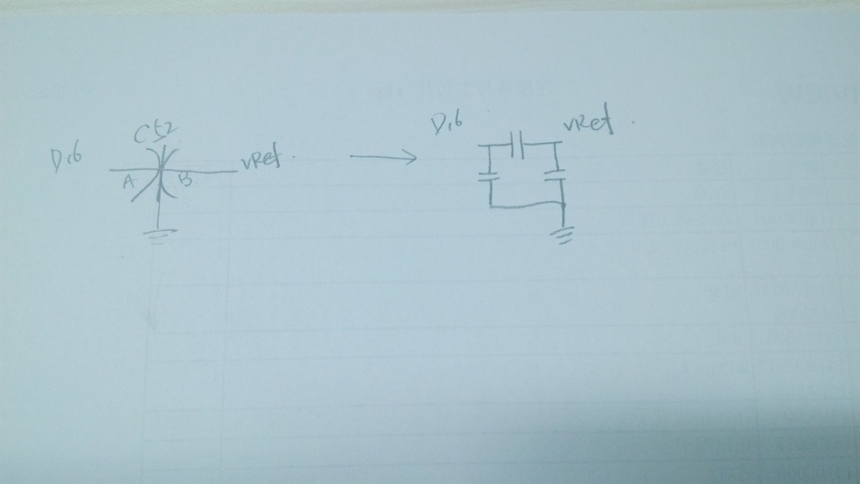
    My question above is, can I use three discrete caps to replace the C52?like below,or just only one cap(between D16 cathode and vRef)? 

    Otherwise, according to "x2y filter&decoupling capacitors"(the datasheet of C52),The X2Y component contains two shunt or “line-to-ground” Y capacitors.There is "GND" surround(between) each A & B electrode,it seems that you can't achieve AC couple between the D16 cathode and the vRef by use this X2Y capacitors(be shielded by GND)? It  just contains two low ESL and balanced Caps provide unequaled high-frequency working performance.

    Regards. 

  • Zuan,

    The reason for using X2Y capacitor is, as you said, to get very good high frequency performance at higher capacitance values. The extra capacitance to the ground is just a "side-effect". To do the minimum, you just need to connect a capacitor with good frequency response between D16 and vRef.

    Regards,
    Subhash
  • Hi,Subhash
    Can you provide me with some reference about LED drive circuit?(Like 4715S or 4232)

    Regards,
    Zuan

  • Hi Zuan,

    Sure I can give you reference for driving LEDs. Can you tell me your input supply voltage? It would help to know more about your application in general.
    Also, to keep the posts relevant, can you please start a new thread in this forum?

    Regards,
    Subhash

  • Hi,Subhash
    Please reply to the new post:"OPT8241&OPT9221:Reference circuit for driving LEDs".
    Thanks.

    Regards,
    Zuan