This thread has been locked.

If you have a related question, please click the "Ask a related question" button in the top right corner. The newly created question will be automatically linked to this question.

CCS/IWR1443: IWR1443 uniflash

Part Number: IWR1443
Other Parts Discussed in Thread: UNIFLASH,

Tool/software: Code Composer Studio

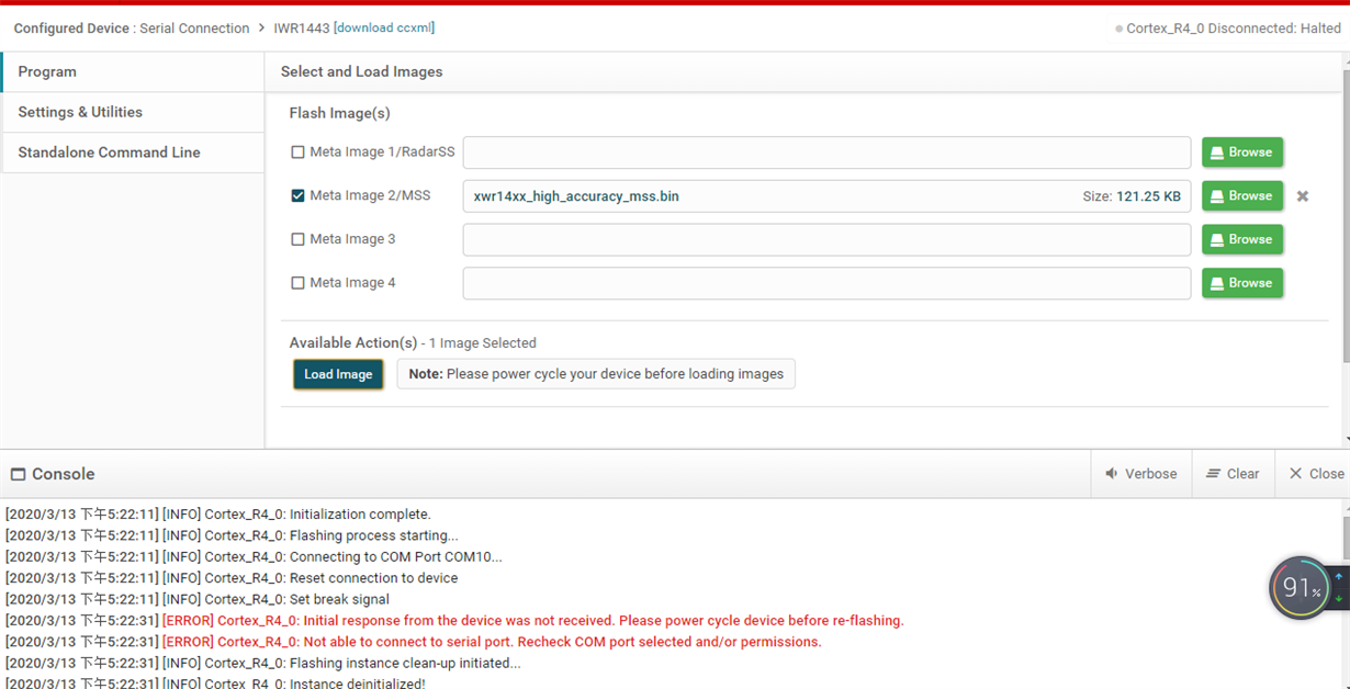
Provide all power(3.3V、1.8V、1.3V、1.192V) to IWR1443.My IWR1443 is not load code using Uniflash. Please help me to check my Schematic of IWR1443. Are there any error. Please help me to correct them.

8507.IRW1443.pdf

  • Hello user4206174,

          For connecting to Uniflash, Device need to be kept in the Flash programming boot mode and need to apply reset to register boot mode.  Then UART ports would be available for the Uniflash tool 

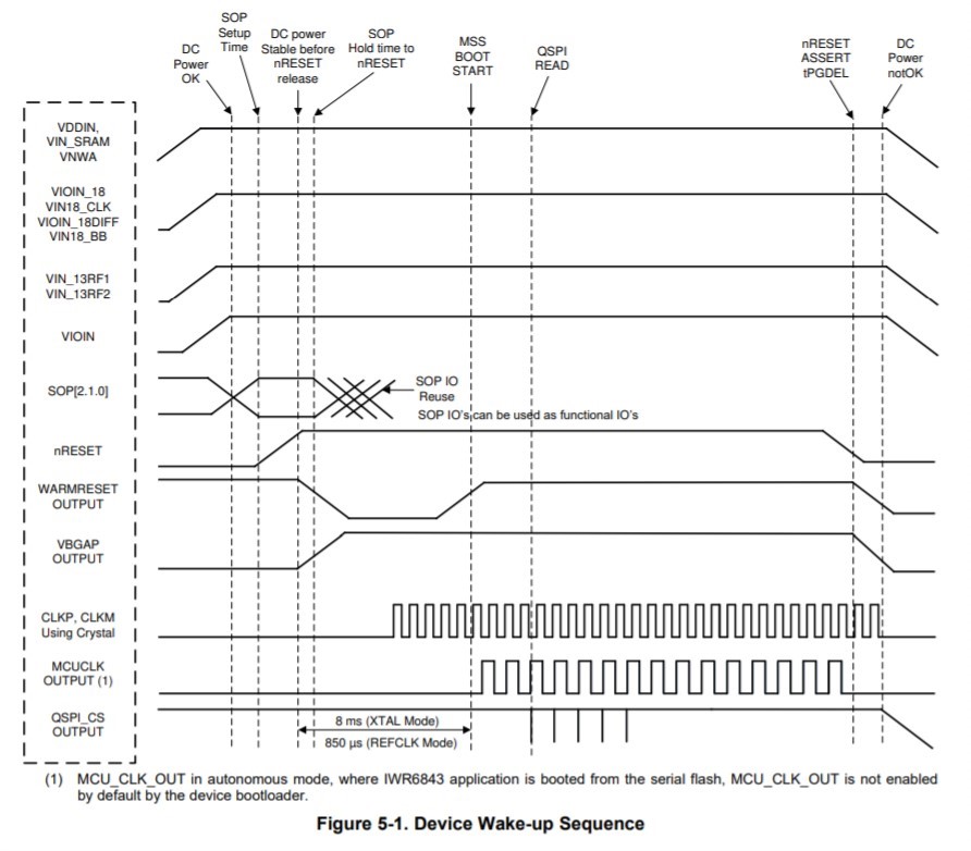
    Also you need to ensure all the power supplies are stable and SOP lines are right boot mode configuration before releasing nreset line as shown in the below diagram. 

    If there is any fault in the hardware (Power supply, Clocking, Flash connectivity etc.) , NERROR pin would be asserted. Do you see this being asserted? 

    Thanks and regards,

    CHETHAN KUMAR Y.B.

  • Set SOP0=1、SOP1=0、SOP2=1.VBGAP is 0.8V 、 VOUT_14APLL1 is 1.41V、VOUT_14SYNTH is 0V、VOUT_PA1 is 0V(No R13)、VOUT_PA2 is 0V(No R13)、NRESET is 1.6V in flash programing mode。

    IWR1443 connect to uniflash with JTAG of XDS110 DEGBUG PROBE,VBGAP is 0V 、 VOUT_14APLL1 is 0V、VOUT_14SYNTH is 0V、VOUT_PA1 is 0V(No R13)、VOUT_PA2 is 0V(No R13)、NRESET is 0.1V in flash programing mode.

    Set SOP0=1、SOP1=0、SOP2=0.VBGAP is 0.8V 、 VOUT_14APLL1 is 1.41V、VOUT_14SYNTH is 0V、VOUT_PA1 is 0V(No R13)、VOUT_PA2 is 0V(No R13)、NRESET is 3.14V in functional mode。

     I measure all power(3.3V、1.8V、1.3V、1.192V) with oscilloscope. All the power supplies are stable.

    NERROR_IN pin is 3.3V, NERROR_OUT Pin had no lead, NERROR_OUT pin is not measured.

    Please help me to check my Schematic of IWR1443(file).In Schematic SOP0=1、SOP1=0 is fixed. If there is any fault. Please help me to correct them.
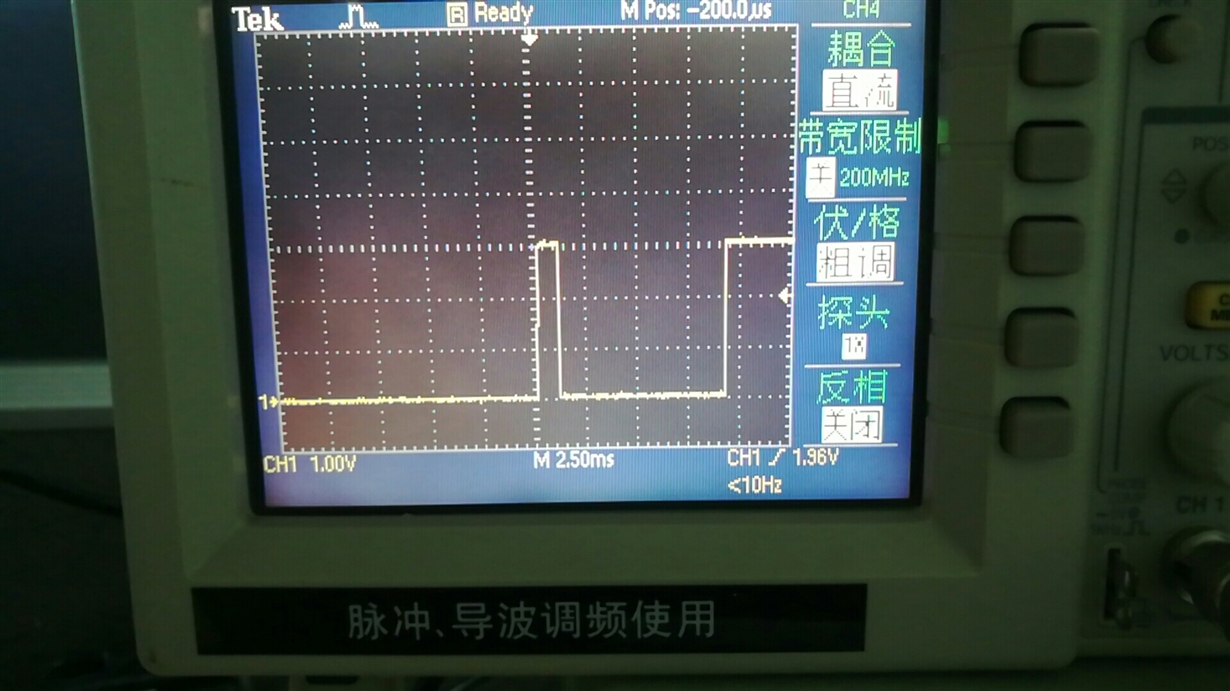
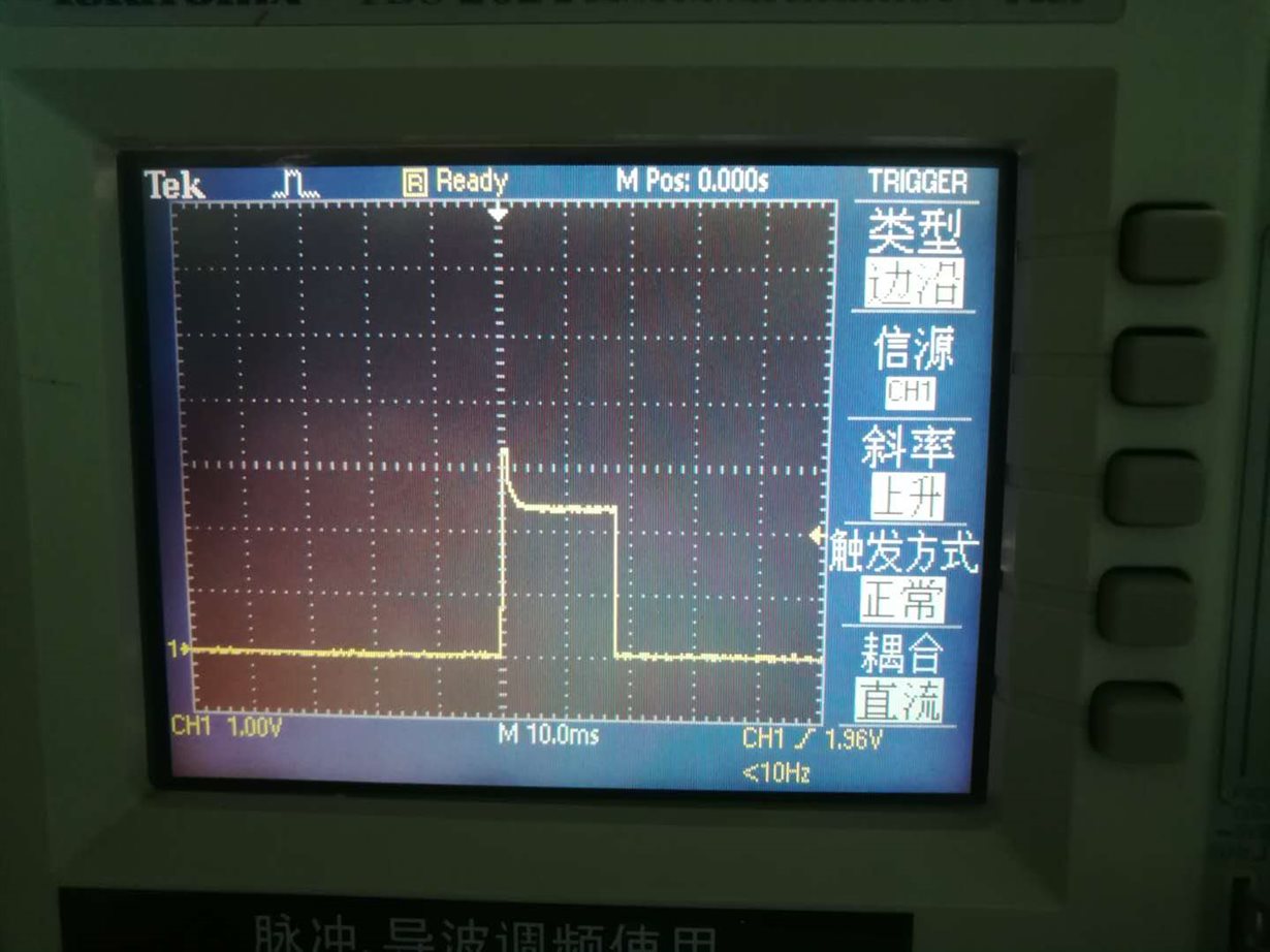
    SOP2 power up  timing sequence

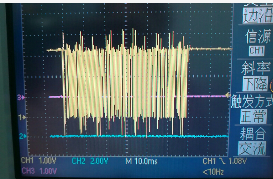
    warmreset power up  timing sequence

    Thank you!!

    SOP2 pull up 3.3V, but P13 PIN(PMIC_CLK_OUT) all is 0V. Please help me.

    Thanks and regards,

    4721.IRW1443.pdf

  • I can flash program to IWR1443 on Circuit board produced.But IWR1443 boot up,but it stop working at once. 

    I can flash program to IWR1443 on EVM(IWR1443Boost), IWR1443 work normal. I use xwr14xx_high_accuracy_mss to flash.

  • Hello user4206174,

        There is another thread https://e2e.ti.com/support/sensors/f/1023/t/890063, Hence this is a duplicate thread for the above question 

    Let us continue the discussion on the above thread. To avoid confusion i will close this thread. 

    Thanks and regards,

    CHETHAN KUMAR Y.B. 

  • I am able to flash the  xwr14xx_high_accuracy_mss application on Circuit board produced,but don't run. IWR1443 is 964FC on Circuit board produced

    I am able to flash and run the xwr14xx_high_accuracy_mss application on EVM(IWR1443 boost). IWR1443 is 964FC on EVM(IWR1443 boost).

    Thanks and regards,

  • Hello user4206174,

        Few comments on the observation. 

    1) Bandgap voltage need to be close to 0.9V (Bandgap voltage is high impedance node, could get loaded with probe). One need to measure with high impedance probe. 

    2) QSPI flash device used is different from that of reference EVM. Please use the same flash device as that of EVM. 

    3) NRESET cannot be different between flashing mode and functional mode. It is driven from externally, Please check this.

    After the SOP lines are configured to default functional mode, Nreset need to be asserted so that boot mode could be registered. 

    4) After the boot mode is registered, you would notice device would start reading from the QSPI flash, And you could see QSPI_CS toggling indicating device is reading from the QSPI flash. 

    5) NERROR_OUT line is open drain output, it needs pull up to 3.3V. Currently it's not connected. 

    6) SOP2 line should be held low in functional mode, could you check why it's goes high and low.? 

    Thanks and regards,

    CHETHAN KUMAR Y.B.

  • 1) Bandgap voltage need to be close to 0.9V (Bandgap voltage is high impedance node, could get loaded with probe). One need to measure with high impedance probe. 

    We measure Bandgap voltage on my EVM and our  Circuit board produced, Bandgap voltage is same almost.

    2) QSPI flash device used is different from that of reference EVM. Please use the same flash device as that of EVM. 

     QSPI flash device used is different. We use MX25L3233FM2I.

    3) NRESET cannot be different between flashing mode and functional mode. It is driven from externally, Please check this.

    We use JTAG to link IWR1443.

    After the SOP lines are configured to default functional mode, Nreset need to be asserted so that boot mode could be registered. 

    4) After the boot mode is registered, you would notice device would start reading from the QSPI flash, And you could see QSPI_CS toggling indicating device is reading from the QSPI flash. 

    5) NERROR_OUT line is open drain output, it needs pull up to 3.3V. Currently it's not connected. 

    NERROR_OUT is out port. There should be no impact .

    6) SOP2 line should be held low in functional mode, could you check why it's goes high and low.? 

    SOP2 line is all low in functional mode.Circuit board produced don't run. Please help me.

    Thanks and regards,

  • Hello,

       Could you please use the Flash device, same as that present in the EVM?

    In the above oscilloscope screen shot "SOP2 power up" shows going high and low why? It should be held low in functional mode. 

    Thanks and regards,

    CHETHAN KUMAR Y.B.