This thread has been locked.

If you have a related question, please click the "Ask a related question" button in the top right corner. The newly created question will be automatically linked to this question.

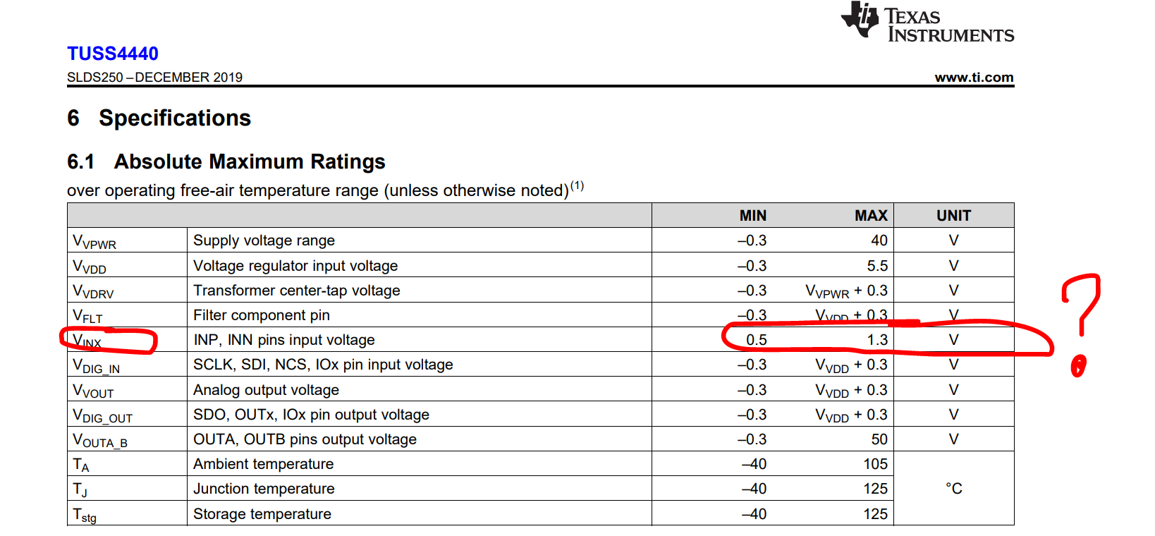
TUSS4470: Wrong absolute maximum ratings on Vinp pin ?

Part Number: TUSS4470

Hello

I am evaluating the TUSS4470 chip, I am using it with a transformer and have voltages in the magnitude of +-200V at transformer secondary winding output. The schematics is similar to TI's eval kit.

In the Eval kit  Vinp is connected with the transformer via R=330pF and R=200ohm in series.

At the same time the TUSS4470 datasheet limits Vinp range to  0.5 - 1.5 V in the absolute maximum ratings. 

In reality given that there is +-200V on the transformer output, it feels like built in protection diodes taking all the beating in the TUSS4470, voltage on Vinp is -diode drop to Vdd+diode drop, and the current reaches 50 mA. That feels like a little too much for the built protection diodes to me, even though it is just several pulses and the diodes somehow manage not to evaporate.

So what is the actual Vinp input current and voltage maximum capability ?  Do I need to use extra protection?  Any guidance from TI ? 

Input impedance of the Vinp input will also be good to know!

Thanks

Dmitry

  • Hi Dmitry,

    The receiver current will be limited by the C_INP cap. The impedance is set by this capacitor with the following equation:

    INP_Impedance = R_INP + [ 1 / ( 6.28 * f_burst * C_INP ) ]

    The max current will be calculated as peak voltage during burst over this impedance. This current into INP should not exceed 15mA. For example, assuming you are using a 40kHz transducer at +/-200V, the current at 40kHz with 330pF CINP will be ~16.6mA through C_INP. You could slightly reduce the value of C_INP to further reduce the current through the INP pin.

  • Akeem

    Thank you for your message.

    Your response suggests that i was probably right and it is the built in ESD diodes of the TUSS4470 inputs that protect the input during the burst. 

    I am a little puzzled with the 15mA you are suggesting as TI's guide on this topic suggests that the max current through the built in ESD diodes in TI chips should not exceed 10mA - see https://e2e.ti.com/blogs_/b/analogwire/archive/2015/12/02/what-you-need-to-know-about-internal-esd-protection-on-integrated-circuits

    By the way, in your formula you added real resistance and capacitive reactance. Normally one would expect the impedance of the RC in series to be Z=SQRT(R^2 + (1/(2*pi*f*C))^2)

    Also these formulas are only good for sinusoidal signals, while we have pulses on the transformer output. 

    In my application f=150 kHz and to get the burst current to the safe levels I would need to reduce the capacitance to below 100pf. It seems like a little too low fro the actual reception.

    I would still like to know the input impedance of the chip's LNA (not the one of the external RC network). If you can kindly provide this information that would be great. A simplified schematics of the input stages of the LNA could be of great help here. 

    Thanks again

    Dmitry

  • Hi Dmitry,

    I am unable to share the internal schematic of the analog front end because it is TI proprietary, but I can confirm we are using internal circuitry that is equivalent to parallel back-to-back diodes to clamp the excitation voltage at INP pin rated for a maximum sink current of ~15mA. This circuitry is not to be confused with traditional IC ESD diodes. Note, the internal current limiting circuitry also relies on the external C_INN value to properly limit current received at the input, which is why it is crucial to use the datasheet's Table 20 equation #2 to calculate the value C_INN based on the transducer frequency. In your case of 150kHz, C_INN=28.3nF (you can round up to a standard value).

    Given you have a +/-200V transducer output, I suspect you are using the TUSS4470 in the pre-driver mode with a transformer. As you've noted, the formula's assume sinusoidal signals, which the transformer still generates during the burst phase at the transducer. There are no square waves at the secondary of the transformer output. We have excited transducers at +/-200V without the need for additional protection at INP, so you should have no complication when using C_INP=330pF, R_INP=200Ohm, and C_INN=28.3nF. The need for additional protection or C_INP recalculation usually becomes relevant for an excitation voltage of 1kV or more.

  • Akeem

    Thank you for your comments.

    I am using external mosfets to drive my transformer and thus i do not have current limitations on the primary side and thus I have square waves on transformer inputs and output. 

    It is still sad that the input resistance of the LNA remains mystery. Usually it is expected to be published in IC specs. It's good to be able to calculate how adding external networks is altering amplification.

    Thanks anyways.

    Dmitry

  • Dmitry,

    The input impedance will vary as a function of input frequency, whereby the input impedance decreases as input frequency increases. Here are some of the approximate input impedance values across frequency:

    Input Frequency (kHz)
    40
    100
    200
    300
    400
    500
    600
    700
    800
    900
    1000
    INP Input Impedance (kΩ)
    500
    180
    80
    50
    32
    22
    15
    13
    10
    8
    7

    One variable omitted was the effect of the transducer’s impedance.

    Note: the INP is biased internally at 0.9V with a 1.5Mohm.

  • Thanks, this is helpful !