This thread has been locked.

If you have a related question, please click the "Ask a related question" button in the top right corner. The newly created question will be automatically linked to this question.

AWR2243: where to find AWR2243 Regmap_Appendix?

Part Number: AWR2243
Other Parts Discussed in Thread: AWR1243, TIDEP-01012, LMK00804B

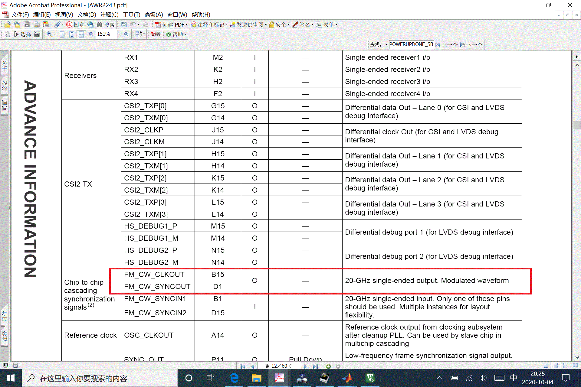
hello, I am designing one image radar and evaluate AWR2243, I download some materials from TI website about AWR2243, but I can't find the detailed Regmap_Appendix,could you provide it to me, so I can read register and configure it through SPI to realize the function I want?

just like the attachments of NXP provideTEF810x_User_Manual_Regmap_Appendix_v0.22.pdf

  • Hello Zheng,

    The Register space for AWR2243 is same as that of AWR1243. So you could refer to the AWR1xxx TRM for that purpose.

    Regards,

    Ishita

  • hello 

      thanks so much for your quick response!

      you mean the AWR1xxx TRM? it is programmer guide for AWR1XXX and AWR2XXX? I download this material from website,but I don't see the detailed register describe? could you send me the materials you mension?

  • hello ,

       I am designing the plan based on AWR2243, I want to use 4 pcs AWR2243+FPGA solution, LVDS(not CSI-2) between AWR2243+FPGA. so I need to configure AWR2243 properly first. could you give me one examples? thanks so much!

  • Hello Zheng,

    Sorry to mention about a wrong document previously. 

    AWR2243 is smart sensor device that can be configured and controlled by external host over SPI interface via API calls.

    These API calls are covered in "mmWave_ICD" i.e the Radar Interface Control Document available in  mmWave Device Firmware Package (DFP).


    The following offerings cover the Device Usage/Interaction/Control view:

    Device Data Sheet : AWR2243 Single-Chip 76- to 81-GHz FMCW Transceiver

    Control/Configuration API details: mmWave Device Firmware Package (DFP).

    mmWave API code for external host :  mmWave Software Development Kit (SDK)

    Sensor configuration and Data path configurations are covered in following documents:

    Programming Chirp Parameters in TI Radar Devices

    AWR1xxx Data Path Programmer’s Guide

    Device AWR2243 has CSI interface available for getting Raw ADC data from Sensor and LVDS for debug. The ICD will guide you through that as well.

    Hope this helps. Please let us know if you have more questions.

    Regards,

    Ishita

  • Hello Ishita Kochar

        one question: you say LVDS for debug, could I getting Raw ADC data from LVDS? my solution is AWR2243+FPGA, LVDS is more convenient for use. thanks!

  • Hello Zheng, 

    Yes you can. Please refer to the mmWave SDK User's Guide on how to enable raw ADC output through LVDS. 

    Regards,

    Ishita

  • Hello Ishita Kochar

       another question: I can't find impedance from datasheet of AWR2243 of receiver/transmitter, the center frequency of my product is 79GHz. I find the impedance of 20G sync signal is 50ohm(the datasheet gives), but I can't find impedance of receiver/transmitter. could you give your great support? thanks so much!

  • Hello Zheng,

    The TX and RX line trace impedance should also be matched to 50 ohms for optimal matching.

    Regards,

    Ishita

  • hello Ishita Kochar,

       thanks! you mean receiver (input impendance) and transmitter(output impendance) of 79G both 50ohm, is it right?

  • hello Ishita,

        another question: I find  77G line width of TI demo(TIDEP-01012) is 0.213mm ,the impendance is 61ohm, if according to 50ohm, the line width should be 0.299mm. could you tell the reason? thanks so much!

  • Hello Zheng,

    The impedance of the receiver / transmitter along with the transition on the PCB (ball to PCB connection with GND vias etc.) provide an S11 of better than -10dB (50 ohms impedance). You can refer to the EVM layout for the ball to PCB transition.

    Regards,

    Vivek

  • Hello Zheng,

    The RF trace is not a mircostrip  but grounded coplanar waveguide. Have you accounted for that in your impedance computation? These traces are matched to 50ohms impedance. Also you need to account for 79Ghz frequency.

    Regards,

    Vivek

  • Hello Zheng,

    To add to what Ishita mentioned, the AWR2243 device abstracts out all the controls in the form of APIs from the host rather than providing low level register controls. The internal firmware within the device then does the appropriate register settings. These drastically easies/simplifies the host SW development, especially for complex scenarios/configurations.

    As Ishita mentioned, the mmwave DFP package provides all the drivers needed on the host side to program the AWr2243 device. The interface Control document ( https://software-dl.ti.com/ra-processors/esd/MMWAVE-DFP-2G/latest/exports/mmWave-Radar-Interface-Control.pdf) lists in detail all the APIs available in the device with descriptions about all the parameters.

    Regards,
    Vivek

  • hello vivek,

       thanks for your answer!

          the line width is 0.299mm based on 50ohm impendance based on 79G, epsilon is 3.16 after I communicated with Rogers because we used R3003G1 5mil. the EVB line width is 0.213mm. I see epsilon of rogers 3003G1 5mil EVB of TI used is 3.0. but even used 3.0, impendance based on this line width is 61.86ohm, not 50ohm.  so this confused me. could you check it again? 

  • Hello Zheng,

    How are you computing the impedance of 61.86 ohms? Have you run the simulations including the ground strip around the RF trace? Have you considered the air dielectric above the copper?

    Regards,
    Vivek

  • Hello vivek,

       I don't simulate include the ground strip around the RF trace because the model is complex, so the line width of demo calculate impedance should be more right. another question: demo is 4 pcs AWR2243 cascaded, the 20G FWCW SYNC output from master is two output: one is for master/slave, another is for two slave based on Wilkenson Power Divider, if my image radar needs more TX/RX(that means the chips I need is more than 4 pcs), how can I use 20G FWCW SYNC? it only 2 output.

  • Hello zheng,

    >>I don't simulate include the ground strip around the RF trace because the model is complex, so the line width of demo calculate impedance should be more right

    Yes, simulating with the GND plan and GND vias around the RF trace will give you a more accurate impedance. That is how we have arrived at the trace width.

    >>another question: demo is 4 pcs AWR2243 cascaded, the 20G FWCW SYNC output from master is two output: one is for master/slave, another is for two slave >>based on Wilkenson Power Divider, if my image radar needs more TX/RX(that means the chips I need is more than 4 pcs), how can I use 20G FWCW SYNC? it >>only 2 output.

    More more the 4 chip cascading you can use an onboard amplifier of the 20Ghz signal and then have larger number of dividers (either a 1:4 divider or two cascaded 1:2 dividers) to derive signal for more chips. You just need to take care that the path delays are matched to all the chips.

    Regards,
    vivek 

  • Dear Vivek,

       thanks for your quick response!

       two questions:

       1. More more the 4 chip cascading you can use an onboard amplifier of the 20Ghz signal and then have larger number of dividers (either a 1:4 divider or two cascaded 1:2 dividers) to derive signal for more chips. You just need to take care that the path delays are matched to all the chips.

        -----onboard amplifier, I don't find this amplifier from schematic released in TI website for cascaded solution. could you give more detailed information, it is one chip or integrated by AWR2243?

    2. for PMIC_CLK_OUT  of AWR2243, how much is the frequency? could it be set by register? the recommended DC/DC for cascaded solution is LP87524, the input frequency range is from 1M~24M with 1M step. 

  • Hello Zheng,

    The TI design is for 4 chip cascade where amplifier is not needed. We do not have  a reference design with the amplifier. You could search online, there are multiple companies providing discrete 20Ghz amplifiers.

    The PMIC clock frequency can be programmed using the "AWR_DEV_PMICCLOCK_CONF_SET_SB" API. Please refer to the Interface Control Document for more details on the API (https://software-dl.ti.com/ra-processors/esd/MMWAVE-DFP-2G/latest/exports/mmWave-Radar-Interface-Control.pdf).

    Request you to raise separate threads for questions that are not related to each other.

    Regards,

    Vivek

  • Hello vivek,

       thanks! I will raise separate threads for questions that are not related to each other in the future.

  • Hello Ishita,

       I am designing Cascaded radar(4 pcs AWR2243) schematic now, confirm one thing: for 40M clk, I prepare to use LMK00804B as 40M clk buffer of slave chips as reference design of TI , for LMK00804B, input clk is from A14(PIN) of master, another N9 pin(MCU_CLKOUT) is for FPGA.

        When I read schematic of TI reference design---tidm464, it gives: clk_sel  “1”  OSC_CLKOUT  “0”   MCU_CLKOUT. clk_sel is pin7 of LMK00804B, it should be used for choose single input clk or differential input clk. from my understanding OSC_CLKOUT and  MCU_CLKOUT both single clk. if my understanding is right, then schematic of tidm464 gives wrong information, is it right?(you can see attachments- it is part of tidm464.lists below)

        additionally, from datasheet, my understanding is : if master chips use 40M OSC, then OSC_CLKOUT is 40M.

    MCU_CLKOUT from datasheet is programmable, it can be set through reg and gives different clk output frequency? is it right?

    thanks so much for quick and strong help from TI support team!

  • Hello Ishita,

      miss one:  2243 IO voltage is 3.3V, LMK00804B VDDO support 3.3V,too! if I use one mater chips to supply 40M to other 3 slave chips, why not both VDDO/VDD supply 3.3V, I find tidm464 VDD is 3.3V  VDDO 1.8V?

  • Hello Vivek,

       I am designing Cascaded radar(4 pcs AWR2243) schematic now, confirm one thing: for 40M clk, I prepare to use LMK00804B as 40M clk buffer of slave chips as reference design of TI , for LMK00804B, input clk is from A14(PIN) of master, another N9 pin(MCU_CLKOUT) is for FPGA.

        When I read schematic of TI reference design---tidm464, it gives: clk_sel  “1”  OSC_CLKOUT  “0”   MCU_CLKOUT. clk_sel is pin7 of LMK00804B, it should be used for choose single input clk or differential input clk. from my understanding OSC_CLKOUT and  MCU_CLKOUT both single clk. if my understanding is right, then schematic of tidm464 gives wrong information, is it right?(you can see attachments- it is part of tidm464.lists below)

        additionally, from datasheet, my understanding is : if master chips use 40M OSC, then OSC_CLKOUT is 40M.

    MCU_CLKOUT from datasheet is programmable, it can be set through reg and gives different clk output frequency? is it right?

    thanks so much for quick and strong help from TI support team!

  • Hello Vivek,

      miss one:  2243 IO voltage is 3.3V, LMK00804B VDDO support 3.3V,too! if I use one mater chips to supply 40M to other 3 slave chips, why not both VDDO/VDD supply 3.3V, I find tidm464 VDD is 3.3V  VDDO 1.8V?

  • Hello Zheng,

    For cascading purpose we use OSC CLKOUT signal and not MCU CLKOUT since OSC CLKOUT is analog signal and has lower jitter/phase noise.

    This signal is 1.4V level and that is why we have used the differential input of the  LMK00804B buffer by biasing  the CLKm pin at mid point (0.7V).

    The VDDO is set to 1.8V since the CLKp can take max of 1.8V input level.

    Regards,
    Vivek

  • Hello Vivek,

       could I use OSC CLKOUT as input LVCOMS_CLK(pin8) of  LMK00804B? in tidm464, input LVCOMS_CLK(pin8) of  LMK00804B is MCU CLKOUT.

  • Hello Zheng,

    The OSC CLKOUT is a 1.4V level signal, so it cannot be used for the LV CMOS input of the LMK buffer since that expects a 3.3V signal level. You need to use the Clk p input of the LMK00804B buffer as used in the TIDEP-01012 (https://www.ti.com/tool/TIDEP-01012

    Regards,

    Vivek

  • Hello Vivek,

       thanks for you quick response!
      I find SYNC_OUT(P11 PIN of AWR2243) connect LVCOMS input of LMK00804B in tidm464,, that means SYNC_OUT output is 3.3V , but OSC CLKOUT is a 1.4V, is right?the datasheet of AWR2243 don't write it clearly here. 

  • Hello Zheng,

    You are right, the SYNC_OUT is digital signal and hence at 3.3V IO level. OSC CLKOUT is an analog signal and 1.4V level.

    Thanks for pointing out lack of clarity in the datasheet. We will try to made the update to clarify this point.

    Regards,

    Vivek