


TI’s Analog Switches and Multiplexers often add very little propagation delay, and in multi-channel devices this extends to channel to channel skew. In some instances, these parameters are not present in the datasheet, however, with a few simple calculations based off datasheet specifications and loading conditions, these values can be easily approximated.
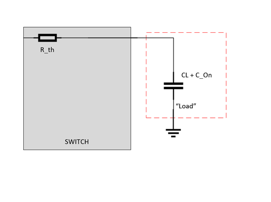
To understand the process, a simplified passive equivalent circuit of the closed switch will be used. This model, shown below, shows the multiplexer as a simple RC circuit when the switch is closed.
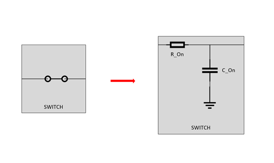
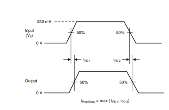
The switch is simply a low pass filter, where RON is the on resistance of the switch (found in datasheet) and the CON is the On-Capacitance (found in datasheet). TI defines propagation delay as the time between when the input is at 50% of final value to when the output reaches 50% of the final value.
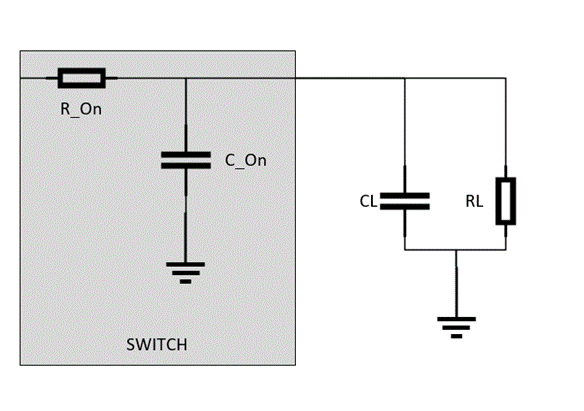
If the switch has no load, propagation delay is going to be approximately 1 RC time constant where R = RON and C = CON. This is going to be very small for most switches – which shows that inherently the switch is generally itself not adding a lot of delay. In most applications there is a load, but in many applications this generic load can be thought of as a RC load to ground.
At first glance the simple RC calculation of a switch without load, RON * CON, approximation is no longer accurate. So, to approximate the propagation delay the circuit must be arranged in a way to where it is essentially 1 RC load again. To do this, first combine the capacitances in parallel. Now define the new “load” as only the combined capacitors.
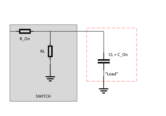
The equivalent resistance feeding into this load is the Thevenin Equivalent resistance – which in this case is simply . This delivers a new RC time constant of RTH * (CL + CON) which is going to approximate the propagation delay of the output of the switch/multiplexer. This method can be used with devices that have propagation delays listed, but the loading conditions are different for the system that the device is being used in as well.
As an example, the propagation delay will be approximated for the TS5A2066 at 3V supply with an RC load of RL = 1MΩ and CL = 20pF. At 3V, the typical on resistance is 12Ω, but can go up to 20Ω. While the on capacitance is 14pF.


Please note that on capacitance does not need to be doubled – the reason there are two values in some datasheets is because the capacitance was measured from different ports, but it is specifying the same parasitic capacitance. Now an upper bound and typical operation point can be found. The loading capacitor is going to be 20pF + 14pF and the RTH is going to ~12 Ohms (typical) | 20 Ohms (max) because RON << RL. This gives an approximate propagation delay of 408ps (typical) and 680ps (upper bound appx.).
If a device has multiple channels there is going to be some skew between the channels – this is often specified less than propagation delay. However, the same steps used to approximate propagation delay can also be used to calculate skew. The skew is a result of changes in propagation delay between channels. To calculate skew, first calculate the propagation delay of one channel as done above. Next look for the on-resistance mismatch between channels, ∆RON in the datasheet, and add/subtract the mismatch value from the RON value and recalculate propagation delay with this new value. The difference between propagation delays is going to be the channel to channel skew.
We’ll continue using the TS5A2066 as an example– its channel mismatch, ∆RON, is typically 0.5Ω with a max of 3.5Ω. Below is the datasheet excerpt for the TS5A2066 showing channel mismatch.
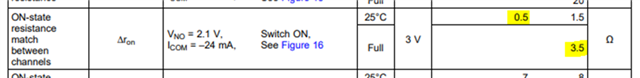
So, this would change RTH to be 12.5Ω (typical) and 16.5Ω (max – assuming other channel is at max on resistance). The new propagation delay would be 425ps (typical) and 561ps (upper bound appx.). This leads to a difference of 17ps (typical) and 119ps (upper bound appx.)
If the system doesn’t follow the typical “RC” load, SPICE simulations with passive elements as a mock up of the load and signal chain can help solve the propagation delay questions for more complicated loading conditions.