


Many of TI’s analog switches and multiplexers do not explicitly state a max allowable junction temperature. At first glance this can seem troubling – but the max junction temperature of the device is respected by following the operating conditions of the multiplexer or switch, and the max operating junction temperature that the device can reach can easily be approximated from available data.
The junction temperature of the vast majority of devices can be broken down into the following form: TJ = TA + RθJA * PDEV . This says the junction temperature (TJ ) is the ambient temperature (TA), plus the thermal resistance from junction to ambient (RθJA), times the power consumed by the device (PDEV). Luckily, the power consumed by an analog switch or multiplexer is simply:

where IDD and ISS are the supply currents, VDD and VSS are the supply voltages, N is the number of active channels, ISW is the current through the switch, and RON is the resistance of the channel. This equation will give the power consumed by the switch at any time. However, to estimate maximum junction temperature, the maximum power needs to be estimated as well. The formula simplifies a bit for max power and is shown below.

This equation is assuming that the device will have max performance in everything to get an estimate of worst-case performance, it should be noted however, that this equation will generally overestimate max junction temperature as all the parameters maxing out at the same time is extremely unlikely for most parts.
Now, it is best to show an example of how this all works.
Example: TMUX1574 | VDD = 5.5V | TA = 125°C
The TMUX1574 is a 4 channel, 2:1 device and it is single supply so ISS and VSS are both equal to zero. At a 5.5V supply the max supply current can be found in the datasheet.
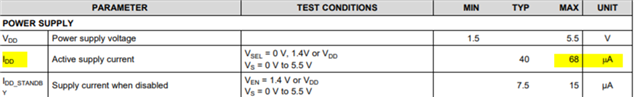
So, this value is going to be 68μA. The device has 4 channels so worst case is that 4 channels are active, so N = 4. Next, the max switch current can be found in the absolute maximum section of the datasheet.
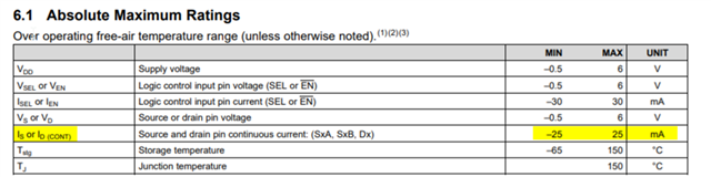
The ISW value is going to be 25mA. Next, look to the specifications to find the on-resistance max at 5.5V.
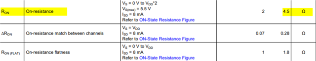
The max on resistance is 4.5 Ω. Now the estimated max power can be approximated:

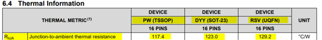
To convert this to junction temperature, it needs to be multiplied by the thermal impedance between ambient and junction and then added to the ambient. The thermal impedance between ambient and junction RθJA is package dependent and found in the datasheet. For the three packages of the TMUX1574, the table is shown below.
With this information, we can calculate the estimated max junction temperature for each package.
PW (TSSOP):
TJ(Max) = 125°C + 117.4 °C/W * 0.011624W = 126.365°C
DYY (SOT-23):
TJ(Max) = 125°C + 123°C/W * 0.011624W = 126.430°C
RSV (UQFN)
TJ(Max) = 125°C + 129.2 °C/W * 0.011624W = 126.502°C
So, even if these devices somehow end up with “worst-case performance”, the temperature added is marginal as most of the temperature is added by the environment, not the multiplexer itself. While using the device under rated conditions, there is virtually no risk of a junction breakdown as the junction shouldn’t heat up much at all during operation (even at worst case conditions).
For more information on thermal metrics please see the following application report: https://www.ti.com/lit/an/spra953c/spra953c.pdf?ts=1639545728909
A calculator has also been created to help with these calculations: Signal Switch Power Dissipation and Junction Temp Calculator