This thread has been locked.

If you have a related question, please click the "Ask a related question" button in the top right corner. The newly created question will be automatically linked to this question.

TMUX1108: Interference when D pin of multiple MUX shorted and cascaded to TIA

Part Number: TMUX1108
Other Parts Discussed in Thread: TMUX1111, TINA-TI, TMUX1112, TMUX6104

Hi Texas

I am looking for a sensor crossbar array (32x32 ie 32 rows and 32 columns) characterization with time-multiplexed fashion. 

Our sensor current which passes through a specific channel (say 1st channel at particular time) of TMUX1108 will vary from 0.1 nA to 100 nA. For safe operation, I have the following queries.

  1. Can I operate the TMUX1108 IC with +/-2.5 supply for rail-to-rail operation ie for input analog of +/-2.5V range or some headroom is required?
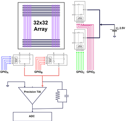
  2. For minimum leakage, and minimum capacitance/parasitic, we are using four TMUX1108 IC to probe 32x32 sensor array (image attached). By mean of enable pin and GPIO we want to characterize (in a time multiplexed manner) a specific sensor among 1024 possible positions in 32x32 crossbar architecture. As attached, will there be any offset/interference/perturbance in multiplexer output if we short D pins of four TMUX1108 (1:16 MUX is shown for representation purpose) and further gives to the input of transimpedance amplifier for measurement of 0.1nA to 100 nA?
  3. At constant temperature and +/-2.5V can we assume that Ron = 125 ohm and 1.5 pF OFF capacitance?
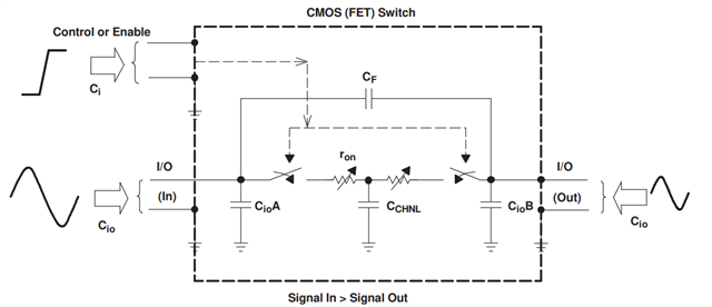
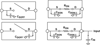
  4. Could you please clarify in detail where exactly these capacitances [CS (Off), CD (Off), CD, CS (On), CIN] are building up when we connect D pin to any of the selectors say S1? For your reference I am attaching one more image, kindly evaluate that.
Thanks and Regards,

Deepak

  • Hey Deepak,

    I'm looking into this. Give me by the end of today and I will provide my feedback.

    Thanks!
    Rami

  • Hey Deepak,

    Sorr for the delay here. 

    Can I operate the TMUX1108 IC with +/-2.5 supply for rail-to-rail operation ie for input analog of +/-2.5V range or some headroom is required?

    Yes TMUX1108 can operate from +/-2.5V rail-to-rail with no headroom required. 

    For minimum leakage, and minimum capacitance/parasitic, we are using four TMUX1108 IC to probe 32x32 sensor array (image attached). By mean of enable pin and GPIO we want to characterize (in a time multiplexed manner) a specific sensor among 1024 possible positions in 32x32 crossbar architecture. As attached, will there be any offset/interference/perturbance in multiplexer output if we short D pins of four TMUX1108 (1:16 MUX is shown for representation purpose) and further gives to the input of transimpedance amplifier for measurement of 0.1nA to 100 nA?

    Shorting the output of 4 muxes will short the other off drain capacitance together as well. Assuming 1 channel turned on and the other 31 are off, you'll see (31*60pF + 65pF) 1925pF or 1.925nF capacitance on the output. This will greatly reduce the bandwidth of the device as well. The leakage will also increase by the same proportion. So your 0.01nA would be 0.31nA typical. You could try to reduce the leakage and capacitance that is accumulated by using 8 of the TMUX1111's instead. It'll be more devices but this big increase in off-capacitance is something that is hard to work around when looking to short devices together to make something like a 32:1 mux. 
    Another recommendation to keep leakage low would be to guard your rails ( see : Guarding in Multiplexer Applications)


    At constant temperature and +/-2.5V can we assume that Ron = 125 ohm and 1.5 pF OFF capacitance?

    I'm not sure where you're getting these values from. TMUX1108 has atypical RON of 2.5ohms and capacitance of 65pF. 


    Could you please clarify in detail where exactly these capacitances [CS (Off), CD (Off), CD, CS (On), CIN] are building up when we connect D pin to any of the selectors say S1? For your reference I am attaching one more image, kindly evaluate that.

    So three of these images are correct but the last one is not. CIN is the capacitance on the control input. 

    Another key distinction here would be the image with CS(ON) and CD(ON). The datasheet can be a little confusing here but the on-capacitance listed is the total CON. So while we typically model this with CS(ON) and CD(ON) on each side of the switch, the 65pF isn't multiplied by two. You can think of it being shared across the two caps. So 32.5pF each for a total of 65pF.

    Let me know if this was all clear and if there's anything else you may need!

    Thanks,
    Rami

  • Hi Rami

    Thanks for the detailed clarifications. I have one more doubt related to the timings of switching operations: Could you please clarify the following, it will be of great help:

    1. How is the RC delay of the switch calculated? Is it RON (source-drain resistor in ON state) multiplied by total CON (effective capacitance from multiple ICs) ? or it is RON + RL multiplied by total CON (effective capacitance from multiple ICs) ie will load at drain terminal plays any role in the switching dynamics? (test circuit attached)
    2. Say TMUX is operating with bipolar supply +/-2.5V, are we supposed to drive the guard rings with precision opamp where non-inverting input of opamp is forced to VSS of TMUX ie -2.5 V ? or non-inverting input of precision opamp has to be grounded?
    3. if a square pulse of 10 mV, 30 nsec passes (S to D or D to S) through TMUX1108 alone (one IC) of switches, how much maximum distortion in input pulse can happen due to switch parasitics?
    4. Frequency domain analysis: Distortions in nsec pulses (square to triangle) will be because of the lowest frequency poles? Is there a way to compensate for the effect of these poles by introducing zeros in the transfer function? Implementation of the same is bothering me…!
    5. TINA-TI spice model for TMUX1108 is not available however IBIS model is provided by TI which is going very difficult to simulate, even I could not find a single source that helps me to import IBIS model in “updated LTSPICE, TINA”…!

     test circuit to characterize the MUX IC.

    Thanks and Regards,

    Deepak

  • Hi Rami

    I have a follow-up question on parallel capacitance calculation due to shorting of multiple ICs.

    ************* pasting your solution********************

    Shorting the output of 4 muxes will short the other off-drain capacitance together as well. Assuming 1 channel is turned on and the other 31 are off, you'll see (31*60pF + 65pF) 1925pF or 1.925nF capacitance on the output.

    ******************end***********************************

    will this calculation be valid even if "we disable 3 ICs, enable 1 channel of 1st IC is ON" ie contribution of parasitics when ICs are disabled with GPIOs?

    Thanks and Regards,

    Deepak

  • Hey Deepak,

    How is the RC delay of the switch calculated? Is it RON (source-drain resistor in ON state) multiplied by total CON (effective capacitance from multiple ICs) ? or it is RON + RL multiplied by total CON (effective capacitance from multiple ICs) ie will load at drain terminal plays any role in the switching dynamics? (test circuit attached)

    The load definitely plays a role and often times will be more of a determining factor in timing than the actual switch. Since timing specs are often taken at the 10/90 of the output relative to when the input hits 90/10, you for sure need to account for the RCload. You can look in the Overview of the test setups in the datasheet to get a better understanding (section 8.1).
    Additionally, we have a good FAQ on how to calculate this as well, in case it helps make things clearer : [FAQ] How do I Approximate Propagation Delay and Channel to Channel Skew in an Analog Switch/Multiplexer?


    Say TMUX is operating with bipolar supply +/-2.5V, are we supposed to drive the guard rings with precision opamp where non-inverting input of opamp is forced to VSS of TMUX ie -2.5 V ? or non-inverting input of precision opamp has to be grounded?

    The idea here is to get the trace and guarding to be the same potential so grounded the opamp input should get you there, otherwise you'd be adding a bias. 

    if a square pulse of 10 mV, 30 nsec passes (S to D or D to S) through TMUX1108 alone (one IC) of switches, how much maximum distortion in input pulse can happen due to switch parasitics?

    Is 30nsec the pule width? I believe question 1 covers this. It would be load dependent here but if we pretend that it's going into a high impedance node with no capacitive loading (ie only the device RC having an effect), we can estimate this by using the max RON and CON (~5ohm and 65pF). I come up with 3.25ns. How you're defining the distortion will matter on where you want to measure from. Fro example, If you're looking for the 90% output then 2*tao(your RC constant) would be about there. If you're wanting the 50 to 50 swing then 1RC would be enough. 
    To truly estimate the distortion the load would be necessary though and in a lot of cases the mux won't be nearly as impactful. 

    Frequency domain analysis: Distortions in nsec pulses (square to triangle) will be because of the lowest frequency poles? Is there a way to compensate for the effect of these poles by introducing zeros in the transfer function? Implementation of the same is bothering me…!

    What are you defining as distortion here? If you're concerned with the bandwidth or the propagation delay I'm not sure if there is a good way to introduce zeros in the transfer function to reduce this. What type of signals do you plan to actually pass through the mux (ie frequency, voltage)? Based on the above it seems you're looking for 10mV @ 33MHz. I'm a bit skeptical that using 4xTMUX1108 would work here. The BW of just one device is 90MHz. Adding the off-capacitance of the off channels of 3 others would be pushing the limits since when the off capacitance is a bit higher and when you tie the outputs together the bandwidth would greatly reduce. You may want to test this out yourself on your board before finazlizng any layouts.  

    TINA-TI spice model for TMUX1108 is not available however IBIS model is provided by TI which is going very difficult to simulate, even I could not find a single source that helps me to import IBIS model in “updated LTSPICE, TINA”…!

    A new IBIS model is in queue and will be released by the end of the year. The PSPICE for TI model is also in queue for development but in the meantime, you can create the model using passive components. See [FAQ] What if my Analog Switch/Multiplexer is Missing a PSpice Model?

    will this calculation be valid even if "we disable 3 ICs, enable 1 channel of 1st IC is ON" ie contribution of parasitics when ICs are disabled with GPIOs?

    I actually have had a huge oversight on this. Sorry for the confusion here but you wouldn't add all 8 signal paths from each device. The outputs would only see the drains, so you would just need to add 1 CD(OFF) from each device present. So in the case of the 4xTMUX1108 you would only add 3 CDOFF's and then 1x(CON). So your capacitance would actually be 65 (CON) + 3x60 (CDOFF) = 245pF.
    If you went with the TMUX1111 you would need 8 devices so 17(CON) + 7*10 (CDOFF) = 87pF. I would still think here that the TMUX1111 would be pushing it on meeting your needs but would offer the best chance of success. 

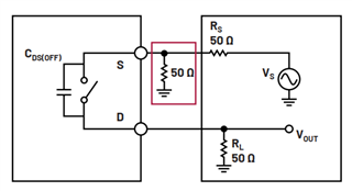
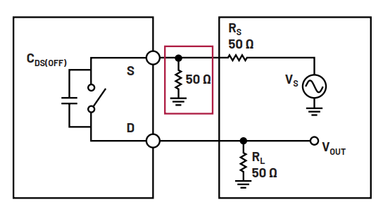
    Another thing to note is that this image does not look quite correct for CDS(OFF)

    What you've modeled is the feedthrough capacitance (sometimes labeled Cpd or CF). It should be two different parasitic caps to ground, as you previously drew. Here's another image that may help make things clear.


    Thanks,
    Rami

  • Hi Rami,


    Thanks. Seems I have to follow your suggestion of using TMUX1111 however I am not able to digest the calculations (if we use 8 TMUX1111 in parallel) that you did for parasitics (CD, CS) ie “17(CON) + 7*10 (CDOFF) = 87pF”.

    This part does not have to enable a pin as well. Could you please clarify it in detail? 

    Also, i would like to go with TMUX1112 (Normally open or off) as it is more closed to my requirements.

    Thanks

    Deepak

  • Hey Deepak,

    Thanks for double checking that math! Seems I only added 1 channel per device instead of 4, as it's a 4ch 1:1 and my math was for a 1ch 4:1. Unfortunately this would actually be much higher than anticipated. TMUX111x would also provide too much capacitance if we were to tie all the drains together. 
    This is a tricky ask and we may not be able to find something that would limit the capacitance at this +/-2.5V rail while also being a precision device. 
    What are the specific criteria you have to work with? Is there a max RON you're looking at? and can the rails be higher than +/-2.5?
    If  we can use rails at a higher voltage and if this is going into a higher impedance pathway (as your op amp should be) so RON has some room to budge could the TMUX6104 work for you here? It's typically a mid-voltage (up to 36V) but if we can use at least +/-5V rails this could be a solution. The higher the rail voltage the better the performance though. Just something to keep in mind. 

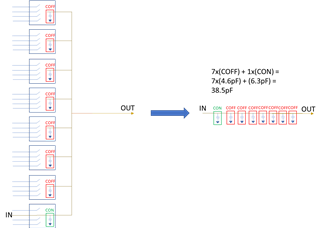
    I'm getting 38.5pF on this one. I've gone ahead and added a very high level image of how I'm getting this, just to make sure that I'm clear and double check myself this time.


    Thanks,
    Rami

  • Hi Rami,

    My supply budget now is 0-5V.

    TMUX 6104 is ruled out for following reasons:

    1. Ron is very high

    2. very slow channel switching time

    my analog design change is: High frequency pulse (25 MHz to 40 MHz) —> SPDT —> 1:32 Demultiplexer—> sensor array (32x32) —> Multiplexer—> Transimpedance amplifier.

    Goal is to route the precise amplitude (100 mV), precise pulse width (50nsec to 500 nsec) through a specific sensor. 
    we can’t afford huge capacitance and series resistance.

    clean transition with minimal loss is expected.

    could you please suggest the best possible solution.?

    also for tmux1111 worst case capacitance calculation that offer clean path

    Thanks

    Deepak

  • Hey Deepak,

    If you're going through a SPDT, then a 32:1 demultiplexer created from smaller switches, then the array then another multiplexer into the TIA I feel you'll have a hard time to reduce the capacitance enough to operate at 40MHz. 
    Additionally, you'll won't be dealing with just accumulated capacitance and resistance, you'll also be dealing with leakages as well. 
    You would be better off using more TIA's and reduce the mux count. You'll want to minimize how many components you're signal is going through if you're so concerned with precision. Going through 3 mux stages along with all the parasitics involved (board, pin & IC level) will greatly reduce BW and increase leakage which decreases precision. You also are increasing the trace length here which is something you'll also want to minimize. 
    Maybe you can find a middle ground in how many TIAs vs muxes? Is there a reason you need to only use one amplifier? 

    Thanks,
    Rami

  • Hey Rami,


    Thanks. I can redesign my experiment where leakage current can be minimised to 20 nA max, and i hope leakage will be still in the said limit. My requirement is to measure current through one channel however other channels (total 31 number of column among 32 channels) will be in high impedance state. Implementing of multiple TIA ie parallel column current sensing will be huge deviation from the set goal. Minimising the trace length is still a major problem..!


    Thanks

    Deepak

  • Hey Deepak,

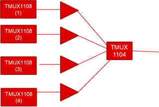
    Well the idea here would be to use muxes on both sides to try and isolate and reduce the loads on both sides of the amp. Basically you could use 4 TMUX1108 where the 8 signals would have an associate TIA. Then from there you would mux those 4 TIA outputs to your signal measuring pin. I drew a quick drawing below. Here, the signal can still be measured through a signal channel, which is your requirement. TMUX1108 and 1104 will also have enable pins here which I believe was requirement. 


    Would this solution work for you?

    -Rami