Other Parts Discussed in Thread: TXB0108, TXB0102, TXS0102
Hello TI Team,
I would like to inquire about the feasibility of the following concept or seek expert advice on suitable TI product models.
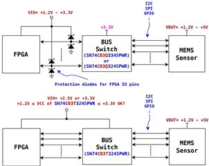
We have a new project that involves using an FPGA to access MEMS Sensors with different voltage levels. In order to protect the FPGA's IO pins and switch IO signals, we are considering adding a Bus Switch between them, such as SN74CB3Q3345PWR or SN74CB3T3245PWR, as shown in the two diagrams below.
1. Since SN74CB3Q3345PWR is a rail-to-rail switch, it may damage the FPGA pins when VDUT voltage exceeds the FPGA's VIO voltage. Therefore, we need to add a clamp diode to the signals between the FPGA and SN74CB3Q3345PWR to protect the FPGA pins.
2. The maximum voltage output of SN74CB3T3245PWR is limited to VCC. If we supply VIO voltage to both the FPGA's IO and SN74CB3T3245PWR simultaneously, can we eliminate the previously mentioned clamp diode?
3. The recommended range for SN74CB3T3245PWR VCC is only 2.3V to 3.6V. If we set its VCC to 1.2V or 1.8V, can the bidirectional signals between the FPGA and Sensor still be transmitted normally? Additionally, can it limit potentially excessive voltages to within 1.2V or 1.8V to protect the FPGA pins?
4. SN74CB3T3245PWR is suitable for high-to-low voltage IO applications. If the FPGA's VIO voltage is 3.3V and VDUT is 5V, can it correctly transmit bidirectional signals?
Thank you in advance for your suggestions.