This thread has been locked.

If you have a related question, please click the "Ask a related question" button in the top right corner. The newly created question will be automatically linked to this question.

TS3A27518E: Eliminate false ON of NC, NO, and COM when starting up the power supply (Vcc)

Part Number: TS3A27518E

Tool/software:

Dear Specialists,

My customer is considering TS3A27518E and has a question.

I would be grateful if you could advise.

---

Since the pull-up power supply for the SD card signal line comes up before the SD card's VDD, I am considering using the TS3A27518E as a solution.

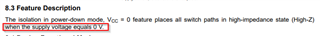
At this time, I want to eliminate false ON of NC, NO, and COM when the power supply (Vcc) is turned on.

According to the datasheet,

① The input pin ratings of the TS3A27518E are specified in 6.1 Absolute Maximum Rating on p. 5 of the data sheet.

VNC, VNO, and VCOM are specified as voltage values, but they also apply when the power supply is turned off.

There is no risk of damage if they are within the range of -0.5 to 4.6V when the power supply is turned off.

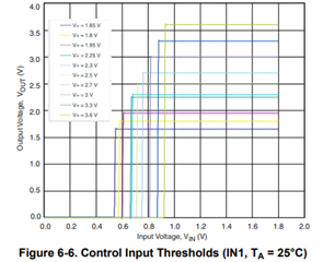
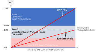
② Figure 6-6. Control Input Thresholds (IN1, TA = 25°C) on p. 12 of the data sheet shows a graph of control voltage and output characteristics.

Although this is a graph of IN1, IN1, IN2, and /EN are specified with the same characteristics in the electrical characteristics, so they can be considered to be the same.

When V+ = 1.65V, it can be confirmed that the output voltage changes from around 0.53V when the control voltage is 0.53V.

The EN threshold is between VIL and VIH, which is significantly lower than 1.65V,
so it is possible that NC, NO, and COM may be turned on.

Based on ① and ②,
I think that if EN is connected to a power supply of 1.2V or higher and power is turned on at Vcc, there is no possibility that NC, NO, or COM will be turned ON.
Is this understanding correct?

If you have any other solution to Eliminate false ON of NC, NO, and COM when starting up the power supply (Vcc), could you advise?

ーーー

I appreciate your great help in advance.

Best regards,

Shinichi

  • Hello Shinichi,

    1. We do not recommend using the device within its absolute maximum ratings. This can cause damage to the device. 

    The TS3A27518E has the power-down feature that whenever the device is off all of the switch paths are in high impedance mode. So when the supply is off the is no signal passing through the device and no damage will be caused.

    2. So according to the graph you mentioned (as seen below) with Vcc = 1.65V at ~0.6V the IN pin is going to toggle high and we will see an output signal, which in this case is 1.65V. 

    While the 0.6V might seem as the threshold for the control pin to toggle the switch, I believe it is in the unknown region of VIH and VIL. We have an FAQ about it explaining what is that unknown region and what does it mean, but I will also explain below. 

    In the example shown below the case is with Vcc = 1.8V. The red region is that unknown region I mentioned earlier, which means while the IN pin is in that voltage range. The switch behavior is not predictable. So when we spec VIH and VIL we provide some breathing room to guarantee device behavior. As shown in the capture below the VIH can be at 1.17V, but we can't really guarantee that every device in that case will toggle high so there is extra breathing room provided and the VIH will be specked at 1.35V instead to guarantee device behavior. Same idea with the VIL case, but the opposite. 

    This whole explanation was for to basically say that while 0.6V does toggle the device on, it is not a guarantee and probably ~0.85V is where the actual VIH spec is.  

    So to your question, the device is enable low, so if there is a 1.2V signal on the EN pin then NC, NO, or COM will not turn ON. 

    Your understanding is correct. 

    Thanks,

    Nir

  • Hi Nir,

    Thank you for your reply.

    I understand TS3A27518E has a power down feature.

    On the other hand, I don't think this function is guaranteed to prevent false ON until VCC starts to rise and reaches the set voltage. Is this understanding correct?

    If so, I think it would be effective to use a method where EN is input at 1.2V so that NC, NO, or COM are not falsely turned on when the power is turned on.
    What do you think?

    Could you please advise?

    I appreciate your great help and cooperation.

    Best regards,

    Shinichi

  • Hello Shinichi,

    There seems to be a slight misunderstanding. The power down feature makes all switches paths to be in high impedance mode when Vcc = 0V, not when its sets to some voltage. 

    For clarification, can you please elaborate on what will the voltage level on the input of the device before the supply voltage settles? At least an estimate?

    From my understanding you will have a voltage input on the mux greater than the supply, because the voltage on the supply won't settle fast enough to match the input voltage; which might cause a false on. If that is the case then I can recommend the TMUX2889. It can pass signals greater than its supply up to 5.5V. 

    Thanks,

    Nir 

  • Hi Nir,

    The customer would like to use for SD card interface.

    Since the pull-up power supply for the SD card's signal line comes up before the SD card's VDD, we are considering using the following switch as a countermeasure.

    1. We do not recommend using the device within its absolute maximum ratings. This can cause damage to the device. 

    When the absolute maximum rating is specified as a voltage, the device should not be damaged even if the power is turned off.

    With other devices, there are many cases where signals are input when the power is turned off.

    Why is the TS3A27518E the only one that does not allow this type of usage?

    Could you please check with the designer.

    I appreciate your great help and cooperation.

    Best regards,

    Shinichi

  • Hello Shinichi,

    In general we don't recommend using our devices under absolute maximum conditions. But as you mentioned: "When the absolute maximum rating is specified as a voltage, the device should not be damaged even if the power is turned off." - you are correct because of the power-down feature the device has.

    Signals can be inputted to the device while its turned off without the risk of damaging it, since the switch paths go into high-impedance state. 

    Thanks,

    Nir 

  • Hi Nir,

    The customer has  an additional question.

    Could you please advise? 

    ---

    I understand that up to Vcc 1.65V, it is high impedance because it is in power-down mode.

    When Vcc and /EN are input from the same 3.3V power supply, is it possible that NC, NO, and COM will be ON from the time the power supply rises until Vcc reaches 1.65V (despite /EN threshold 1.15V)?
    On the other hand, in this condition, is it possible to understand that NC, NO, and COM are high impedance?

    I would like to confirm that if the power supply rise speed is slow, whether the device will turn ON and NC, NO, and COM will be ON even if Vcc is below 1.65V, which is outside the operating voltage.

    --

    I appreciate your great help and cooperation.

    Best regards,

    Shinichi

  • Hello Shinichi,

    Power-down mode is activated when Vcc = 0. If Vcc > 0, then the device is not in power-down mode anymore and the device is not in high impedance. I want to clarify that and make sure there is an understanding. 

    The TS3A27518E is an enable low device, meaning in order to enable the switch a signal of 0V (low) needs to be sent to the enable pin. NC, NO, and COM will not be on if a positive voltage signal is sent to the EN pin. 


    IN1 and IN2 have different logic though.

    Thanks,

    Nir 

  • Hi Nir,

    Thank you for your reply.

    I classified it into four areas based on the VCC voltage (0 to 3.6V).

    Could you please confirm and advise?

    ---

    Area 1: VCC0V: NC and COM are high impedance.

    Area 2: The device does not operate from 0V to a certain voltage.

    Area 3: There is an area where the device actually operates at voltages below the operating voltage (1.65V).

    Area 4: Within the operating voltage range (1.65V to 3.3V): Operates as specified in the data sheet.

    TS3A27518E Start Up.pdf

    What the customer would like you to confirm the operation of Area 3.

    Could you please advise?

    (1) The power supply voltage of the TS3A27518 is specified as 1.65V to 3.6V,
    but the device actually turns ON somewhere in Area 3 (up to 1.65V).

    (2) When VCC and EN are connected, VCC and EN rise at the same time.
    EN is definitely in the H state when the device starts to operate.

    (3) Therefore, it is thought that all channels will be high impedance if VCC = EN even in Area 3.

    Please let me know if there is a reason why these assumptions (1) to (3) are not met.

    ---

    I appreciate your great help and cooperation.

    Best regards,

    Shinichi

  • Hello Shinichi,

    We can't guarantee device behavior outside of the recommended voltage range.

    Area 3 in question is in the range outside of the recommended operation spec. I can't provide solid answers since the device behavior is unpredictable at that voltage range. 

    1. The device might turn on below the recommended range, this is something that we can't predict.

    2. This might happen, but again we can't guarantee device behavior outside the recommended operating range. 

    3. Again, this might occur but we can't predict it.

    Thanks,

    Nir 

  • Hi Nir,

    Thank you for your reply.

    I understand there is no guarantee the outside of the recommended voltage range.

    I'll share the information with the customer.

    I appreciate your great help and cooperation.

    Best regards,

    Shinichi