Tool/software:
HI ,
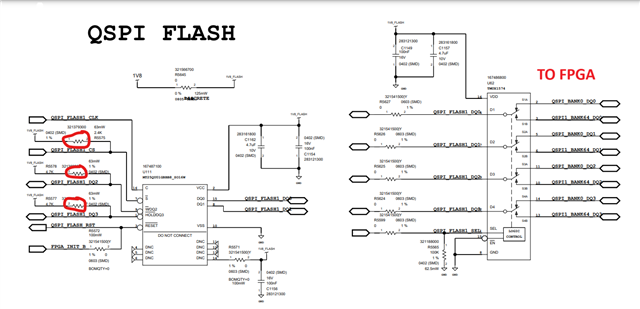
We are using TMUX1574 mux in our design. One end of the mux (Drain / D side) is connected to QSPI Flash memory, the other end (Source / S Side) is connected to FPGA Banks. There is a XTP Checklist for FPGA which recommends to connect a pull-up resistor on the Flash Side for (Chip select, DQ2,DQ3).Since it is not an end to end connection (FPGA to Flash Memory).
I have attached an image FYR. Kindly check and tell.
1. Do we require a pull up resistor on the (Source / S Side) of the MUX?
2.Can you share the Internal architecture diagram (Whether it is a MOSFET or any other switch used) of the MUX ?