This thread has been locked.

If you have a related question, please click the "Ask a related question" button in the top right corner. The newly created question will be automatically linked to this question.

TS5MP646: TS3DV642 "Alternate"

Part Number: TS5MP646
Other Parts Discussed in Thread: TS3DV642, TS3DV520, TS3DV621,

The packaging of the TSMP64x parts are really tight; I saw as a related answer on this forum that the TS3DV642 may be a suitable part that performs the similar task of bi-directional 1:2/2:1 MIPI CSI-2 switching (data rate of 2.5Gbps).

I wanted to confirm that all of the switch structures inside the part are identical, even those notionally for the lower-speed channels in the device's original application. As a MIPI x4 lane requires 5 differential channels to be switched together, I need to use either the SCL or HPD pins to send the MIPI clock signal. 

Can I apply the Port A and Port B characteristics to every switch in that port, including the SCL/HPD/CEC switches?

Thanks!

  • A few add-on questions:

    1. Are +/- swappable for layout purposes?
    2. Comparable devices have many VDD/GND pins; I have added as many vias as possible to the EPAD to optimize inductance to ground (I assume this is the reasoning as it doesn't dissipate much power), how can I optimize the VCC delivery path besides short via to GND and nearby de-coupling?
    3. In general, can this device be treated as 12 high-bandwidth, fully bi-directional switches where a subset of them are "matched" on-die?
    4. Is there a recommended set of switches to use for a 5th differential pair? SCL/SDA seems best suited for this task judging from device pin-out.

    Thanks!
  • Krunal,

    1. Are +/- swappable for layout purposes?

    2. Comparable devices have many VDD/GND pins; I have added as many vias as possible to the EPAD to optimize inductance to ground (I assume this is the reasoning as it doesn't dissipate much power), how can I optimize the VCC delivery path besides short via to GND and nearby de-coupling? 

    As you recognized this is a low power device and thermal performance isn't as important as signal integrity.  The best thing you can do for the signal integrity on the VCC pin is place the de-coupling caps to ground as close as possible to the IC. 

    3. In general, can this device be treated as 12 high-bandwidth, fully bi-directional switches where a subset of them are "matched" on-die?

    4. Is there a recommended set of switches to use for a 5th differential pair? SCL/SDA seems best suited for this task judging from device pin-out.

    Let us know if you have additional questions.

    Thank you,

    Adam

  • Adam —

    I'd be an absolutely dangerous engineer if I could use the search function! Thank you for those links and prompt reply.

    The links to the referenced threads in the post you linked for my questions 3 and 4 seem to be dead; is there any chance you could help find those? I tried playing with the URLs to see if I could figure out where they went but didn't have any luck.

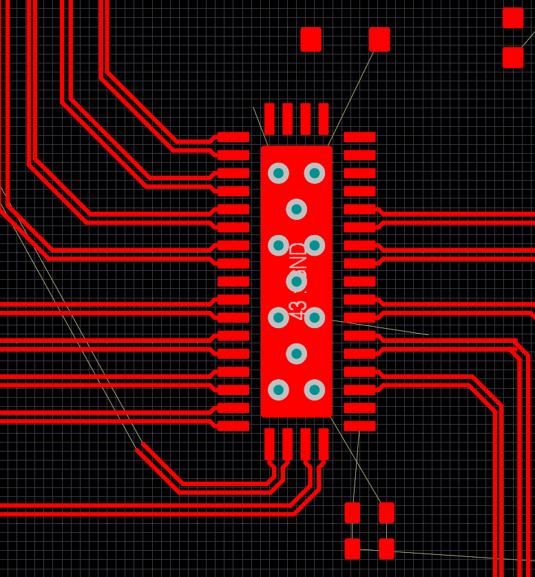
    Just want to read some more details on using the SCL/SDA/HPD/CEC pins to send my 5th lane of MIPI data and then I believe this is all set. The pinout of the device isn't ideal for 5 lane breakout (see attached) but at least I don't need to use blind/buried vias like the smaller part!

  • Nevermind, I managed to figure out where the links went after some sleuthing.

    For future readers / searchers:

    "4 Lane MIPI Swtich, TS3DV641/642, TS3DV520" e2e.ti.com/.../1456958
    "TS3DV642 support LVDS Switch or not" e2e.ti.com/.../305257

    (And another fixed link in case future reader wants to follow it all to the end: e2e.ti.com/.../427561, "TS3DV621 (1:2 video switch) vs TS3DV642 (newer 1:2 SPDT video switch)")

    The forum ID changed from 388 to 391 at some point I guess.

    Adam, my question is on the following comment from what Jared Becker posted many years ago:

    "Also, please note that due to the length of the wire on the SCL and SDA line, there is a propagation delay associated with these lines compared to the data lines."

    This seems to tell me that while being better for my layout purposes, these lines may have a different tpd compared to the other ports? The datasheet reports SCL/SDA/HPD/CEC having an equivalent typical tpd on Port A and being slightly faster on Port B. I saw some other customer posts here utilizing this switch successfully for a MIPI application, but I'm not sure what speed they were at.

    I have PCB layout / other guides telling me I need to be worried about skew at the 5-10ps level, so if I'm running a pair through one of the non-data channels, I may be seeing an amount of skew that will break my link / require some kind of re-timing.
  • Krunal,

    You are correct that the IC layout for a passive FET switch is the biggest factor of propagation delay.  

    I'm more familiar with the TS5MP646 device but have contacted the group that can help with the question about the internal layout of the TS3DV642 and how that will effect the propagation delay.  

    Thank you,

    Adam

  • Thanks Adam, I'm going to pencil it into the design for now but I will keep an eye out for a reply re: that behavior on the TS3DV642.

    I'll also throw a vote into whatever bucket it is that alternate packaging for the TS5MP646 device that doesn't require micro-vias / HDI technology on a PCB would be awesome, but of course I can't tell you how many other people / volume would want the same thing to warrant the packaging and new validation effort since it would no longer be a chip-scale device.

  • Krunal,

    Noted on the TS5MP646 package request. We are currently evaluating if there is enough business to invest in different package options.

    Adam