This thread has been locked.

If you have a related question, please click the "Ask a related question" button in the top right corner. The newly created question will be automatically linked to this question.

CD4051B: CD4051 output has spur while the input is clean

Part Number: CD4051B

Hi team,

My customer is testing CD4051B. The use case is as below. CD4051B VDD=3.3V
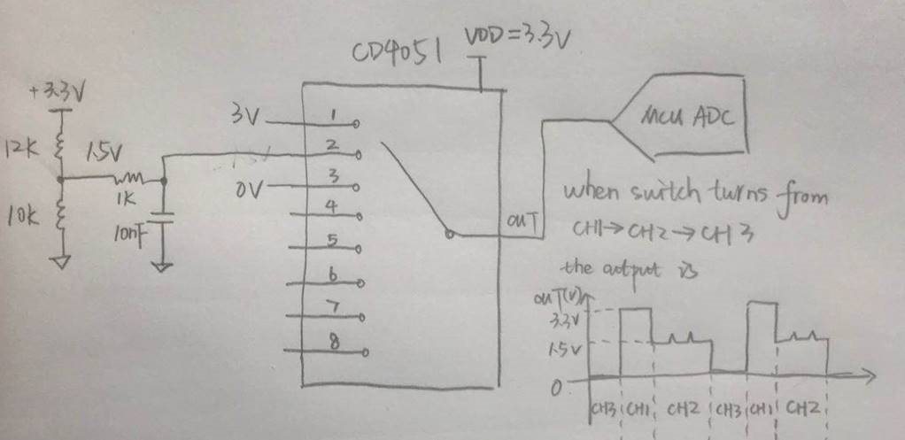
When we switch the input channel from CH1—>CH2—>CH3, the output should be change from 3V—>1.5V—>0V. But we found that when CD4051B switches to CH2 which is 1.5V input, the output shows some spur on top of the 1.5V waveform.  The output real waveform is as below picture and the spur on 1.5V is as the red circle shows.

To verify if the spur showing on output is from input, we measured the input CH2 and output at the same scope. Green is CH2 1.5V which is always stable and Yellow is output. When output is switched to CH2, it raises up from 0V to 1.5V but the spur shows on 1.5V output. When the spur comes up, the input CH2 1.5V is clean.

We zoom in the waveform as  below: you can see the spur on 1.5V output shows up in a very high slew ragte.

What's more, we also have below finding:

1. When CH2 voltage is around 1.5V~1.6V, we will see the spur show up on output when it switches to CH2. But when we adjust CH2 voltage to get it away from 1.5~1.6V, there is no spur on output when it switches to CH2

2. When we change CD4051B VDD to 5V from 3.3V. The issue goes away

So can you help analyze what cause the spur on the output? Thanks.

Best regards,

Wayne

  • Hi Wayne,

    Looks like there is an over-shoot on CH2 during switching – reason being there is not enough break-before-make  causing coupling between signals when switching. There are several ways you can minimize the overshoot:

    • Add a capacitor to the drain/Output pin of the switch- The capacitor value will vary with the amount of overshoot, but may be on the order of 100pF to 10nF.
    • There could be inductance on your signal path that could be creating the voltage spike due to a strong driver causing fast change in current. Placing series resistance could help with the overshoot by weakening the driver strength

    What does the signal look like if you remove the mux and short the signal path?

    These devices were characterized and are tested at 5V,10V and 15V. They can operate above and below that but are not specd there.

    If you are running at 3.3V, .I would also recommend, for an 8:1, 1-channel, 3.3 V supply voltage rail, to use the TMUX1308 in similar configuration and low cost.

    The main difference with operation at 5V supply vs 3.3V is the CD4051B, like most signal switches, on-state resistance will increase as the supply voltage decreases.  The CD4051B has an on-state resistance of 470 ohms with a 5V supply and will be much higher as the supply voltage decreases to 3.3V. 

    Regards,

    Saminah