This thread has been locked.

If you have a related question, please click the "Ask a related question" button in the top right corner. The newly created question will be automatically linked to this question.

TMUX1108: Fail safe

Part Number: TMUX1108
Other Parts Discussed in Thread: SN74CBTLV3251, OPA333, OPA388

Hello TI Experts,

I wanted to confirm the behavior of TMUX1108 and Fail-Safe logic feature 

If I understand correctly, fail safe allows the control pins to be biased upto 5.5V above VSS while supply is OFF (VDD = 0) disconnecting all channels

Quoting the datasheet...
 [This feature allows voltages on the control pins to be applied before the supply pin, protecting the device from potential damage]

However, as per maximum rating source and drain voltages (Vsx, Vd) are limited to -0.5V to VDD+0.5 which means the device does not support partial power down, i.e. VDD = 0

#1) So now I am unclear how fail-safe exactly protects the device and what is the advantage / intended use of Fail Safe feature?

It appears that TMUX1108 negate the need to power down VDD to save power, i.e.
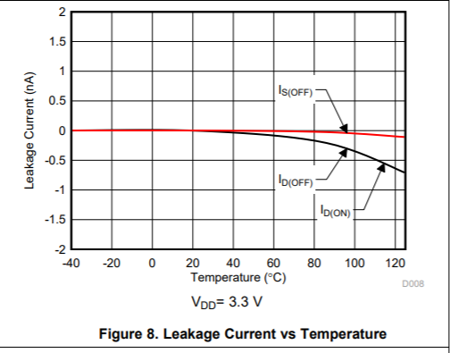
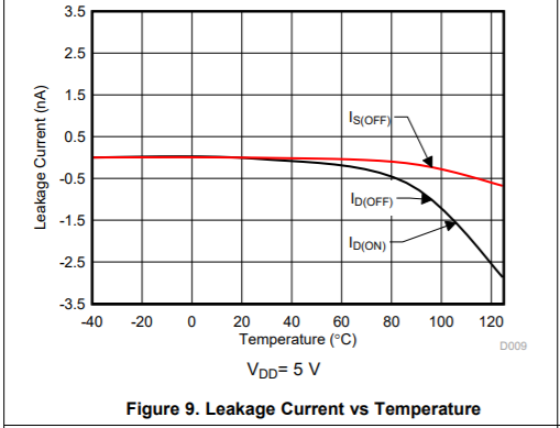
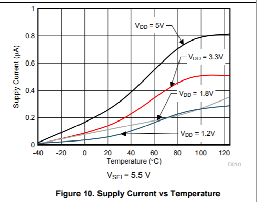
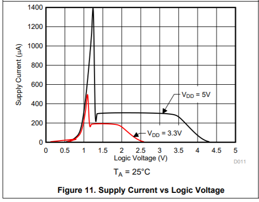
assuming VDD = 5V, maximum leakage / supply current is given 

Is(off) + Id(off) = 5nA 
IDD = 1μA   (Logic Input = 0V or 5V)

#2) what is the worst case leakage and supply currents for Analog inputs 0V ≤ Vsx ≤ 3V?


Best,
AJ

  • The Fail-Safe Logic feature applies only to the control pins (Ax, EN), not to the I/O pins (Sx, D). The datasheet says:

    Fail-Safe Logic minimizes system complexity by removing the need for power supply sequencing on the logic control pins.

    This implies that power supply sequencing is still needed on the I/O pins.

    When a logic input is at a voltage near the middle between VDD and GND, then you get cross currents (see [FAQ] How does a slow or floating input affect a CMOS device?). (Please note that the IDD test condition is overly restrictive; the logic input voltage does not need to be as high as 5.5 V, but can be any voltage at or above VDD.)

    The analog I/Os are not connected to MOSFET gates, are are not affected by the voltage level. There is no logic input test condition for the analog leakage current specification because it does not matter; the specified IS(OFF) and ID(OFF) values are valid for any logic input voltage.

  • Hi Clemens,

    Thank you for the prompt response. I was concerned about device leakage if I/O are biased while device is OFF. 
    However, this use case is not not allowed as the device does not support partial power off

    Best,
    AJ

  • Hi AJ,

    As Clemens Indicated, Fail-Safe Logic only applies to the logic pins. Partial Power Down is a feature that TI refers to as "Powered-Off Protection", but unfortunately these parts do not fall under the precision category like the TMUX1108. 

    For your 2nd question:

    On Leakage: Using the following two graphs from the datasheet you can find your approximated 25C leakage current. This is the typical use case.

    The worst case leakage occurs at higher operating temperatures, to approximate the worst case scenario for leakage use the one of the following two tables below (depending on VDD):

    For supply current, the I/O voltage does not impact supply current, the largest contributing factors to supply current are VDD, Select Pin Voltage (with reference to ground), and temperature. To approximate supply current please refer to the following figures from the datasheet:

    If you have any other questions please don't hesitate to reach out!

    Best,

    Parker Dodson

  • Hi Parker,

    Thank you for the additional information.

    Let me share some background info for our application. I am designing a precision battery powered industrial DAQ system, we have multi-channel / SW configurable input types as shown in the figure below. 


    To save power and extend battery life, analog section would be powered off when inputs are configured as digital inputs and vice a versa.

    Ideally the Analog MUX supports partial power down when Digital inputs are HI, i.e. i.e. SN74CBTLV3251 in my other post :)
    However, as you pointed out they don't fall under "precision" category so I am hesitant to use it...

    Perhaps, I can use a partial-off supported SPST 1:1 switch to break the path before going into the MUX in the case of TMUX1108. Assuming we can live with the added cost / design complexity for control signals, I am afraid this SPST 1:1 offers no benefit over SN74CBTLV3251?

    So it looks like my only option is to use partially-off SPDT 2:1 for each channel and isolate the analog path when it's powered down.

    Best,
    AJ

  • Hi AJ,

    What is the resolution of the ADC in your system?  You may not need what TI would consider a "Precision MUX", I say this because of the buffer after the mux. Usually Buffers are high impedance, so on resistance and leakage most likely won't degrade the accuracy of the signal much. If I am misunderstanding the buffer you are planning to use in the system please let me know. 

    However, one possible fix to your issue is shown below, this will give TMUX1108 a psuedo-partial power down, but there are caveats and challenges when picking the correct FET and power supply:

    There a few factors that you need to consider here. The first being the Rds(on) of the NFET. This will be highest when Vsx = 3V, when referring to the the original range of 0V - 3V that is going into the Multiplexer. If the VDD can be 5V, then the lowest Vgs = 2V. If the max Rds(on) is low then you should be able to block the signals coming towards the mux when Vdd = 0V, and still retain a large amount of the precision when Vdd is active. This prevents damage to the ESD diodes, the part of the IC at most risk during a partial power down event. The trade off is that the switch isn't guaranteed Hi-Z with this method, but voltage won't be passed to the input of the switch either which will negate a lot of the negative effects.

    If you have any more questions please let me know!

    Best,

    Parker Dodson

  • Hello Parker, 

    Thanks for the suggestion. We have a 24-bit ADC, it's more than adequate for the system requirement for 0.1% FS measurement accuracy 
    For the buffer, I plan to use OPA388 or OPA333 but will probably ask on Amplifier Forum for other options. 

    Following this useful discussion, I have decided to place the SN74CBTLV3251 as ON/OFF switch in front of the TMUX1108 to break the signal path and isolate the mux when analog is powered down. 

    Again, thank you for a great support!

    Best,
    AJ