This thread has been locked.

If you have a related question, please click the "Ask a related question" button in the top right corner. The newly created question will be automatically linked to this question.

TS5A3154: Open/short measurement design

Part Number: TS5A3154
Other Parts Discussed in Thread: LM2904, LM334, , TS5MP646

Note.xlsxOPENSHORTV02-20200820.pdf

Hi TI:

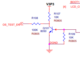
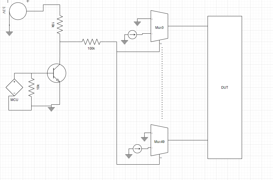
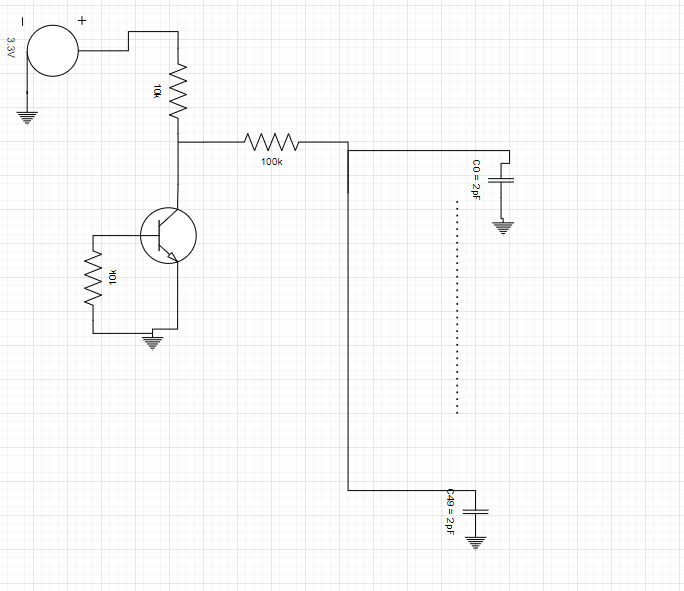
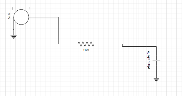
    Hope your support to review the design as attached file,which designed to measurement the voltage of Pinx's D1&D2 for DUT whit -1000uA.

it was design by fixed current source LM334, AMP LM2904,analog switch TS5A3154DCUR,should i use two switch for  everyone pin?

  • Hi Hogan,

    I am a bit confused by the block diagram, and I just want to make sure I understand what you are trying to do.

    In the block diagram you indicate both the ADC and the Current Source is being fed into the switch matrix, where every switch shares a common output with one of the DUT pins. However in the schematic only the Current source is routed to the switch matrix, with the other input being GND. Are these switches only used to turn on / off current into the DUT for the D1/D2 Measurements, or are they supposed to be switching between the ADC and current source? 

    As far as how the the TS5A3154DCUR was wired, there was one possible issue that I saw. All of the active low output enable pins were shorted together; while this isn't a problem per-se, but the issue is that instead of the nominal 2pF of capacitance you have that multiplied by 50. So you have a 100pF of bus capacitance, along with the "R" being ~110k ohms. This leads to a time constant in the micro-seconds, and since this part is active low, the device will be active for microseconds before the design will disable the device. If this isn't a concern for your system it shouldn't matter, but it is something to be aware of. 

    But please let me know some more information about the application so  can see if there is any system changes that need to be made.

    Best,

    Parker Dodson

  • Hi  Parker:

          Thanks you for answering my quetion!

    “Are these switches only used to turn on / off current into the DUT for the D1/D2 Measurements, or are they supposed to be switching between the ADC and current source?  ”

    ----> The analog switches only used to turn on / off current into the DUT for the D1/D2 Measurements, When COM pin connected to the NO pin ,then current fed into the Pinx to D1/D2,the ADC was designed  to sample the voltage of D1/D2 ,then the ADC output to MCU to told the value of voltage. 

    "So you have a 100pF of bus capacitance, along with the "R" being ~110k ohms. This leads to a time constant in the micro-seconds, and since this part is active low, the device will be active for microseconds before the design will disable the device. If this isn't a concern for your system it shouldn't matter, but it is something to be aware of. "

    ------>I will be aware of this issue.If it will affect the function,i will debug the the value of  the R&C .

    The initinal request was that: measure the voltage of D1 and D1 by +/-1000uA .

  • Hi  Parker:

          I can't find the 2pF cap for TS5A3154 in its datasheet, How do you get the 110kohm?

  • Hi Hogan,

    Alright I understand how the switch matrix is supposed to function. I don't see any issue with the current set up you have with respect to the application, and I think the amount of switches you have is sufficient. 

    That being said, please see the following excerpt from the TS5A3154 Datasheet on pages 5,7,9, or 11. 

    The above pictures shows what it is at VCC = 5V, but its typical value of 2pF does not fluctuate with supply voltage, as all spec'd voltage ranges contain this capacitance.

    This is a parasitic cap to ground, and with 50 switches on the same bus it can be approximated as ~100pF typical value.

    As for the 110 K Ohm resistance for the RC please see below:

    From the MCU you have this discrete switch to enable/disable the device. If at start up the NPN is in cut-off you essentially have 2 resistors in series, the pull-up (10 K Ohm) and the 100K ohm resistance, which is the 110 K Ohms. This is connected to the OS_TEST_EN bus, and if you see below:

    All the switches in the matrix are also connected to OS_TEST_EN, this is a digital input, where every input has a 2pF parasitic capacitance with respect to ground. This means your RC time constant is about ~ 11us and to charge the digital input to a disable state would be about 1 time constant (about a 61% charge of the digital input capacitance would be required to disable the device, from the application of the 3.3V VCC signal. 

    But beside that issue, everything else looks fine, and I don't see any other things that I'd expect to cause problems.

    Best,

    Parker Dodson

  • Hi Parker Dodson:

         Thank you for the feedback!

    “All the switches in the matrix are also connected to OS_TEST_EN, this is a digital input, where every input has a 2pF parasitic capacitance with respect to ground. ”

    ---->It means every switch input pin should have a 2pF parasitic capacitance rather than a 0.1nF cap in OS_TEST_EN bus line.

    If i want to use this design board to transfer image signal data with 9.9G b/s(data with MIPI protocol ), what should i have to change?

  • Hi Hogan,

    I think we are on the same page, but just to clarify this is what the current OS_TEST_EN bus's equivalent circuit looks like:

    OS_TEST_EN Bus Before Simplifications

    Remove Voltage Sources that would be 0V. Replace Select Pin with Parasitic Capacitances:

    BJT is in Cutoff (open Circuit)

    Add Series Resistances together and then add Parasitic Caps together and the final simplified OS_TEST_EN bus:

    To reduce delay and increase max frequency going towards the OS_TEST_EN bus line:

    For the OS_TEST_EN, I'd remove the series 100k Ohm resistor, removing this drops the delay by  about ~91%. However you'd still be in the microsecond range. However you still do have a low pass filter with a corner frequency of about 160 KHz with the pull-up. To increase the max frequency to the OS_TEST_EN bus you must either decrease the value of the pull-up and/or separate the Enable into multiple bus's. This pin does not directly impact data rate though. The Enable bus can be slower than the data you are trying to run through the device, once the device is enabled the channels impact the bandwidth more than anything. 

    As for the MIPI modifications I have a couple questions.

    1. What is the maximum frequency going through each switch? because the current switches you are using are only rated (typ) at 100MHz.

    2. I am a bit confused how you are transferring this over to MIPI with this board? Could you possibly elaborate a bit more? There might be better switches suited to the application but I want to make sure I understand how you are trying to switch this board over.

    Best,

    Parker Dodson

  • Hi Parker Dodson:

         Thank you for the feedback again!

    Understand the 2pF and 110k ohm setting。

    1. What is the maximum frequency going through each switch? because the current switches you are using are only rated (typ) at 100MHz.

    ---->I was just use 2 lane for MIPI, so there are data0_N/P, data1_N/P, clk_N/P, totally six switchs to transmission data。it looks like needed to 

           reselect the switch since it‘s BW only 100MHz,do you have proposal components capability?

    2. I am a bit confused how you are transferring this over to MIPI with this board? Could you possibly elaborate a bit more? There might be

        better switches suited to the application but I want to make sure I understand how you are trying to switch this board over.

    ---->You had raise a serious problem: how to transmit data and open /short tests,I aming  ker Dodson:

         Thank you for the feedback again!

    Understand the 2pF and 110k ohm setting。

    1. What is the maximum frequency going through each switch? because the current switches you are using are only rated (typ) at 100MHz.

    ---->I was just use 2 lane for MIPI, so there are data0_N/P, data1_N/P, clk_N/P, totally six switchs to transmission data。it looks like needed to 

           reselect the switch since it‘s BW only 100MHz,do you have proposal components capability?

    2. I am a bit confused how you are transferring this over to MIPI with this board? Could you possibly elaborate a bit more? There might be

        better switches suited to the application but I want to make sure I understand how you are trying to switch this board over.

    ---->You had raise a serious problem: how to transmit data and  open /short test,I am rebuilding the schematic to meet the goal.

  • Hi Hogan,

    We do have 2 specific MIPI switches. They are both 5 lane 2:1 MIPI switches.

    The TS5MP645 has a typical bandwidth of 1.5 GHz

    While the TS5MP646 has a typical bandwidth of 3 GHz, and below you can see the Eye Diagram at 2.5 Gbps per lane:

    Is your total through put 9.9Gbps or is that the throughput for each differential pair?

    Best,

    Parker Dodson

  • Hi Parker Dodson:

         Is your total through put 9.9Gbps or is that the throughput for each differential pair?

    ----> 9.9Gbps / lane 

  • Hi Hogan,

    We don't have a solution that will support 9.9Gbps / lane from our MIPI switch portfolio.

    Best,

    Parker Dodson

  • Hi Parker Dodson:

         May i use other protocol(like: Display port/PCIE.......)Switch IC,which just need have differential channel?

  • Hi Hogan,

    Yes you may use other protocols, as long as you don't need higher than 2.7GHz of bandwidth, that is the minimum frequency we expect out of the switch. But it has a typical frequency of 4.1 GHz.

    Best,

    Parker Dodson