This thread has been locked.

If you have a related question, please click the "Ask a related question" button in the top right corner. The newly created question will be automatically linked to this question.

SN74CBTLV3861: SN74CBTLV3861 unable to meet rail-to-rail performance specification

Part Number: SN74CBTLV3861

Hi,

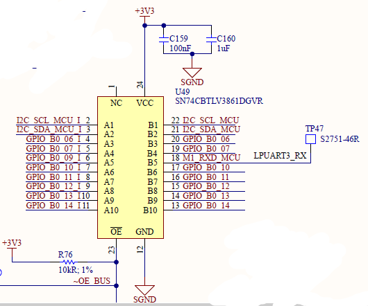
We are using the SN74CBTLV3861 10bit bus switch to isolate our MCU pins from external loads as part of board power-up sequence.

One thing we have recently noticed is that the

We are operating from Vcc=3.3V

Case 1 (switch HighZ):   A1 = open; B1 = pulled-up to 3.3V via 2kR; !OE=high .... then B1 measured reports 3.3V; A1 reports floating

Case 2(switch ON): A1=open; B1=pulled-up to 3.3V via 2kR; !OE=low...then B1 is measured as 3.15V; A1 reported 3.15V

For some reason the bus switch activation is causing the level on B1 to drop from 3.3V to 3.15V. We have noticed this on multiple parts and boards, so damage is unlikely.

Can you help us understand why the voltage drop in Case2 is occuring, even through the datasheet specified 5Ohm pass resistance and rail-to-rail performance?

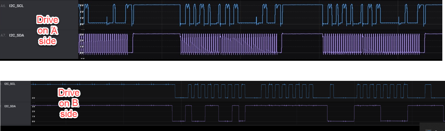
FYI: the application for these pins is I2C (100k/400kbit/s) .

Many thanks!

Simon M.

to isolate 

  • Hi Simon,

    In Case B it seems that the voltage drop isn't occurring due to the switch because A ~ B - this switch in that configuration is drawing a max of +/- 1uA of current due to leakage of the part which wouldn't explain the 150mV voltage drop. Is there anything else on that line that is activated during Case B because I don't think it looks to be the multiplexer due to A ~ B. The voltage drop seen is the result of a ~75uA current being drawn through the pull-up resistor - the Multiplexer will not have that large of current through it when one side of the IC is open circuited unless it is damaged - which I don't suspect to be the problem because of ~0 V across the switch itself.

    That being said - on the note of the Rail to Rail operation. The meaning can be a bit misleading - it means that the switch's don't down-translate, i.e. some of our parts if you have a 5V supply you can only pass up to 3.3V; however if there is current running through the switch there will be a resistance associated with the switch, regardless if it is rail - to - rail or not, and this will cause an insertion loss. However in this application it doesn't seem the switch is what is causing the voltage drop as it seems to be happening over the pull-up resistor.

    All possible current paths should be considered when looking at the pull - ups + what devices could be drawing current in Case B.

    If you could let me know a little bit more about what is on the line and what is active during both cases that would be helpful in looking into what some possible causes of the issue are. Also if possible measuring current going into the switch on the board can help us see if the switch is acting unusual or not.

    Best,

    Parker Dodson

  • Hi Parker,

    Thanks for the reply. In both Case 1 & Case 2, the same secondary I2C devices on the B side of the switch are present, and they are open-drain/collector without any communication. Any leakage from the secondary I2C devices on B side should be present in both Case 1 & 2. 

    In the measurement I mentioned my first post, on the A side of the bus switch we have disconnected our MCU I2C master. Therefore A side is just floating, no pull-ups, no pull-down, just a stub going a connector via a 0R.

    Here is a picture from my schematic showing the signals on each side of the switch,

    Another observation we have made is that bus switch seems to distort the I2C traffic. Below are 2 screenshots where we used a Microchip MCP2221 to drive SCL/SDA from either A side or B side of the switch wit !OE=low, and there is significant cross talk from SCL to SDA.  They are on channel 1 and 2 respectively. I will have more high res captures to share later.

    Your thoughts on this? Is this behavior expected? Should we use separate single channel bus switches e.g. SN74CBTLV1G125DCKR, to avoid this?

    Simon

  • Hello Parker,

    Happy New Year! Do you have any insights to share regarding our observations on distorted I2C signal traffic through the bus switch.

    Thanks,

    Simon

  • Hi Simon,

    Happy New Year to you as well. I am sorry for the delayed response. 

    I understand what you are saying with the voltage drop. If possible could you get a current reading of what is going into the switch at case - I want to see if the device is drawing more current than expected.

    As for the cross talk - this part is a bit older so the cross-talk performance wasn't measured and probably isn't great so a single channel switch may help the solution, but I am a bit wary of this because layout can also affect how lines couple with each other - so layout itself can also create some interference between traces.

    Please let me know if you can get that measurement and also more high res images would be a bit helpful to see if I can see the previous measurements a bit better. 

    Best,

    Parker Dodson

  • Hello Parker,

    We found the root cause of the issue and it did not involve the bus buffer which was a great relief for us. The nets concerned were connected to MCU pins with dual-use boot configuration, and the MCU SOM builder had the default config include a pulldown resistor. This pull-down was rsponsible for the afore mentioned higher than expected current draw and voltage drop as it was in effect "fighting" with the stronger pull-up resistors for I2C. By removing the pull-downs and configuring the MCU eFUSE we could realize normal voltage levels. The cross-talk was isolated to layout and interboard cable routing which had 2 open-drain traces run almost parallel for a significant distance. In upcoming board rev we will address the later. We appreciate support from TI in investigating this matter.

    Best.

    SM