This thread has been locked.

If you have a related question, please click the "Ask a related question" button in the top right corner. The newly created question will be automatically linked to this question.

PROCESSOR-SDK-AM437X: Software crash in "QSPI_BasicExample_idkAM437x_armExampleProject"

Expert 1700 points
Part Number: PROCESSOR-SDK-AM437X


Hello,

I am running the "QSPI_BasicExample_idkAM437x_armExampleProject" in the Processor SDK RTOS AM437x v5.3.0.7 version using CCS 8.3.0.9. The code is running on the AM437x IDK board. The IDK has a QSPI flash on board, which contains 1024 blocks of 64[kB] memory.

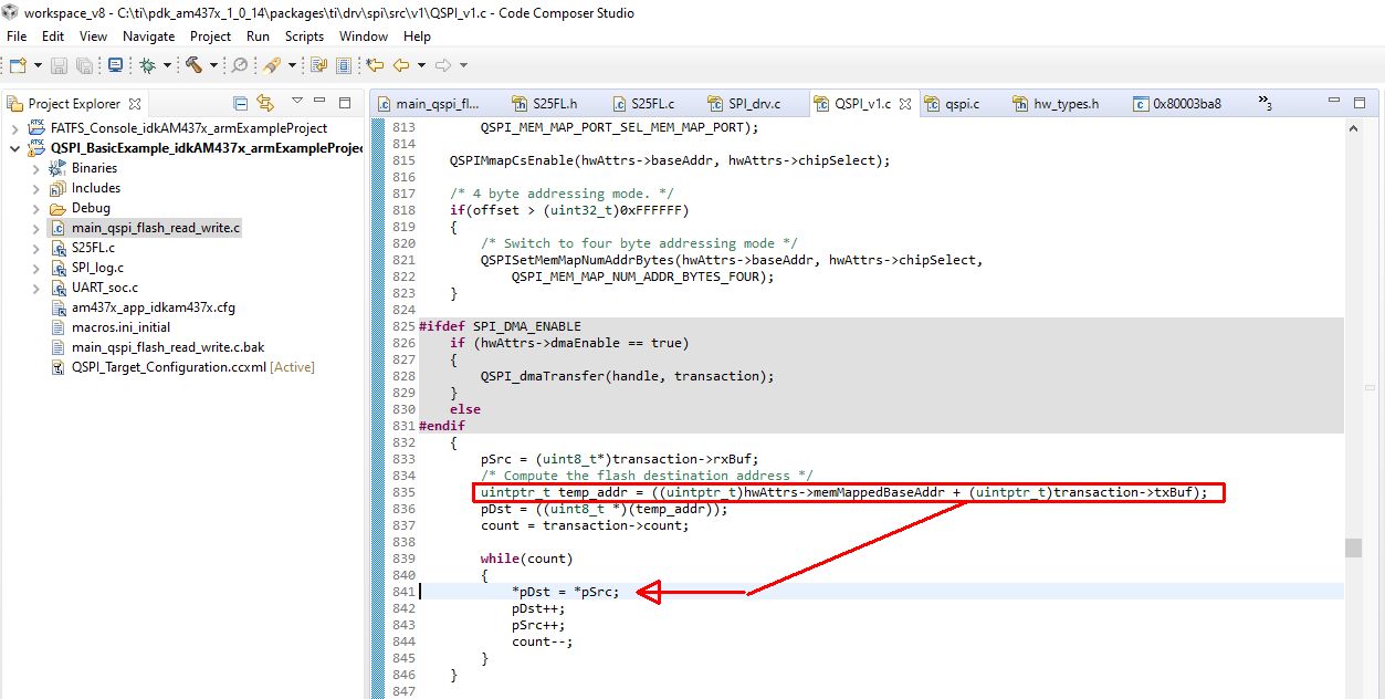
I extended the example code a bit, in order to check if all QSPI memory blocks (from 0...1023) can be accessed. Please have a look at the following code inside red rectangle: 

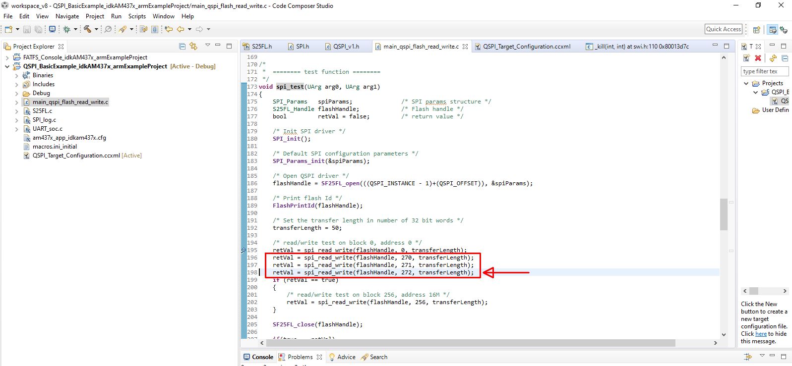
The code seems to crash if I am calling the "spi_read_write()" function for QSPI block 272, see red arrow above and the below picture:


I will try to get closer to the root-cause tomorrow. Is it possible that you quickly check if you see the same behavior on your side?

Thanks,

Inno

  • Hello, I looked a bot further into this issue. This is the function where the software crashes:

    Inside "QSPI_mmap_mode_write_v1" this is the code that leads to the crash:

    It looks like it has something to do with the calculation of the "temp_addr" variable, since obviously "*pDst" points to a forbidden address.

    Thanks,

    Inno

    PS:, even accessing block 16 does not work for me:

    retVal = spi_read_write(flashHandle, 16, transferLength);

  • Hi Inno,

    If you change the value to 64, does it still fail?

    This issue seems to be similar to this thread:

    e2e.ti.com/.../732293

    Regards,

    Dillon

  • Hi Dillon,

    It indeed seems to be connected to that post you mentioned above. If I call the function with block number 64, then I receive:

    CortexA9: Unhandled ADP_Stopped exception 0x80027E68

    Can you please check if the problem appears because I have to use an quite old "SDK RTOS AM437x v5.3.0.7" (I had to temporarily switch to a Win 10 32-bit PC and that one works only with CCS version 8 and therefore I must use an older SDK for a few weeks)? Maybe that issue is already solved in newer SDK versions?

    Maybe it is worth to implement a for-loop in order to check all flash blocks are accessible:

    for(i=0; i<1023; i++) // Flash has 1024 blocks, counting from 0...1023
    {
       retVal = spi_read_write(flashHandle, i, transferLength);
    }

    I may can check on a newer SDK version if that problem persists, but it would be great if you could tell me, which SDK version should have the solution for this issue.

    Thanks,

    Inno 

  • Hi Inno, 

    Currently I don't have access to an AM437x IDK, but I am looking into acquiring one. That way I can run this code and see if I experience the same bug on the newest SDK or not. I'll provide an update in 2-3 days on whether or not I've acquired a board yet. 

    Regards,

    Dillon

  • Hi Inno, 

    I was able to find a colleague that has access to an AM437x IDK, and so I'm going to see if we can run this test tomorrow afternoon.

    Regards,

    Dillon

  • Hi Dillon,

    Thanks for checking this. Please enhance the test a bit, in order to see that you can access each one of the 1024 64kB blocks:

    for(i=0; i<1023; i++) // Flash has 1024 blocks, counting from 0...1023
    {
       retVal = spi_read_write(flashHandle, i, transferLength);
    }

    Thanks,

    Inno

  • Hi Inno,

    I can confirm that the issue is present on the 6.3 SDK. We were able to run the example as is, but the error that you mentioned showed up when testing block 64. I am searching to see if there's a solution, as well as if there's an existing ticket for this issue. If not, I'll file a ticket for it.

    Regards,

    Dillon

  • Hi Dillon,

    Thank you very much for checking this on your side.

    The related E2E that you found (e2e.ti.com/.../732293 was posted in September/October 2018. But the current 6.3 SDK is from April 2020. I wouldn't really expect that a ticket for this topic is open for 1.5 years without progressing. Anyway, hopefully it is not too tricky to solve it.

    I assume the fix will be inside the QSPI driver file "QSPI_v1.c". Would it be possible to get the fix in advance to an SDK release (which may take a while) and we can merge that fix manually to the older SDK version we are using?

    Thanks,

    Inno

  • Hi Dillon,

    we are currently in a process of merging the IDK source code over to our custim board and soon we need to be able to access every flash block.

    Can you please provide an update about this topic? Do you have an idea when we can expect to get the code with the bug fix (we don't need a new SDK release, just the correction in the drivers c/h files)?

    Thanks,

    Inno

  • Hi Inno,

    What mode are you aiming to use when accessing every flash block?

    https://e2e.ti.com/support/processors/f/791/t/732293?pi239031349=2&pi320627=1&pi320966=2)#pi320966=1

    While the E2E thread above does seem to experience a similar issue that we're seeing, that thread did manage to solve the issue in specific scenarios. Have you tried implementing some of the suggestions from earlier in that E2E thread?

    Regards,

    Dillon

  • Hello Dillon,

    regarding the mode:

    I don't really care in which mode I am accessing the flash for a write. I can also change the mode to config (instead of memory mapped) and correct the bugs, which I already found inside "SF25FL_ConfigMode_Write" (missing byte swap, wrong command byte etc.).

    But note that the code crashed already during the write and therefore I did not yet check if I can at least read from all flash blocks. This is something that I can of course test.

    Now to the E2E post, the post that you mentioned above ends with the following lines: 

    "I have not been able to figure out why the first entry is incorrect.
    I read the data back from flash front and backward and still come up with this result.
    Due to this, my thoughts are that the error is in the read.

    I have attached my relevant files with the change so you diff them if you would like.

    Any input on this would be awesome."


    So I am under the impression that there is also a bug for the read and therfore I thought that you are working on fixing the driver when accessing all 1024 blocks in a for-loop in whatever mode (config or memory mapped).

    Alternatively I can try to get the flash write-access working in config mode and cross my fingers that at least the read is working in memory mapped mode. With this approach I may can bypass our current problem.

    Still I would like to know what TI is doing currently in regards to this bug as a previous report from 2018 hasn't been handled until today.

    Thanks,

    Inno

  • Hi Dillon,

    I wrote an own "write to flash" function, which can be seen as a corrected version of "SF25FL_ConfigMode_Write". This own written function works always in standard SPI mode (object->rxLines = QSPI_RX_LINES_SINGLE and object->qspiMode = QSPI_OPER_MODE_CFG). With this function I am able to access all 1024 flash blocks.

    But the TI driver function "SF25FL_bufferRead" also crashes when I try to access all flash blocks. Therefore I have to write an own "read from flash" function, which works in the same way like my "write to flash" function.

    I will share the code with you once I am done. In the meanwhile please let me know if you created a ticket for the bug and in which SDK version this issue will be solved.

    Thanks,

    Inno

  • Hi Inno,

    That's great to hear that you are now able to access all 1024 flash blocks. The ticket, which includes both the SF25FL_ConfigMode_Write and SF25FL_bufferRead bugs, has been created. I do not know which one, but it will be fixed in a future release. And once you share the code, I'll make sure to link it to the ticket as well.

    Regards,

    Dillon

  • Hello Dillon,

    With those read/write functions I am able to access all 1024 flash blocks. I used those functions inside the FATFS example project to copy an application binary and the QSPI SBL binary from the SD card into the QSPI flash device. After a power cycle the IDK booted properly from the QSPI flash.

    Feel free to review and provide feedback as I will not guarantee that there are no further issues. It just looks very promising with those functions.

    /************************************************************************************/
    /* This function is an alternative approach for the TI functions, which allow us    */
    /* to access each of the 1024 (0...1023) 64[kB] memory blocks of the QSPI flash.    */
    /* This function works in the same way like the 'S25FLFlash_BlockErase' or the      */
    /* 'FlashPrintId', which means in standard SPI mode (MOSI/MISO/CLK/CS) accessing    */
    /* the SPI_CORE interface.                                                          */
    /*                                                                                  */
    /* This function has been written because if calling 'SF25FL_bufferRead' when       */
    /* "(QSPI_OPER_MODE_CFG == object->qspiMode)", then there are several bugs inside   */
    /* the function (e.g. missing address byte swap) and if calling 'SF25FL_bufferRead' */
    /* when "(QSPI_OPER_MODE_MMAP == object->qspiMode)", then the QSPI driver crashes   */
    /* when accessing certain flash blocks (addresses), such as flash block 64          */
    /* (address 0x400000).                                                              */
    /*                                                                                  */
    /* See also:                                                                        */
    /* ---------                                                                        */
    /* e2e.ti.com/.../974055                               */
    /* e2e.ti.com/.../969427                             */
    /* e2e.ti.com/.../969166                             */
    /*                                                                                  */
    /*                                                                                  */
    /* Arguments: dstOffstAddr - Flash address to be accessed (0x0...0x3FFFFFF)         */
    /*            dstAddr - Pointer to the buffer where to store that data, which       */
    /*                      has been read from the flash.                               */
    /*            length - number of bytes to read from the flash                       */
    /*            flashHandle - QSPI flash handle                                       */
    /************************************************************************************/
    bool SF25FL_ConfigMode_StandardSPI_Read_IWG(uint32_t dstOffstAddr,
                                        unsigned char* dstAddr,
                                        uint32_t length,
                                        S25FL_Handle flashHandle)
    {
        bool retVal = true;                        /* return value = success */
        bool retVal2 = true; // Success
        SPI_Handle handle = flashHandle->spiHandle; /* SPI handle */
        unsigned char writeVal[4];               /* data to be written */
        uint32_t addrLengthInBytes = 3U;         /* Flash address length in bytes */
        uint32_t readCmd = 0U;                   /* Read command */
        unsigned int frmLength;
        unsigned int transferType;
        uint32_t offsetValue;
        unsigned int operMode;           /* temp variable to hold mode */
        unsigned int rxLines;            /* temp variable to hold rx lines */
        unsigned int rxLinesArg;
        uint32_t tempAddr;
        QSPI_v1_Object  *object;
    
        /* Get the pointer to the object and hwAttrs */
        object = handle->object;
    
    
        /************************************************************/
        /* Stage 1: Save the current mode and rxLine configurations */
        /************************************************************/
        operMode = object->qspiMode;
        rxLines  = object->rxLines;
    
        /**************************************************************************/
        /* Stage 2: Indicate to the QSPI driver to access 'QSPI_cmd_mode_read_v1' */
        /*          upon a read access and 'QSPI_cmd_mode_write_v1' upon a write  */
        /*          access.                                                       */
        /**************************************************************************/
        SPI_control(handle, SPI_V1_CMD_SETCONFIGMODE, NULL);
        rxLinesArg = QSPI_RX_LINES_SINGLE;
        SPI_control(handle, SPI_V1_CMD_SETRXLINES, (void *)&rxLinesArg);
    
        /***************************************************************************/
        /* Stage 3: Identify the number of bytes for the address information, the  */
        /*           proper command byte and set up the total frame length for the */
        /*           QSPI driver.                                                  */
        /***************************************************************************/
    
        addrLengthInBytes = 3U;
        offsetValue = dstOffstAddr; // Load the Flash address to read data from
        if(offsetValue > 0xFFFFFF)
        {
            /* Enter 32 bit addressing mode */
            addrLengthInBytes = 4;
        }
    
        if(offsetValue > 0xFFFFFF)
        {
            readCmd = QSPI_LIB_CMD_READ_SINGLE_4B;
        }
        else
        {
            readCmd = QSPI_LIB_CMD_READ_SINGLE;
        }
    
        /* total transaction frame length in number of words (bytes)*/
        /* This tells the SPI driver for how long to activate the CS signal. */
        frmLength = 1 + addrLengthInBytes + length; // Command byte plus address bytes plus 'length' data bytes
        SPI_control(handle, SPI_V1_CMD_SETFRAMELENGTH, ((void *)&frmLength));
    
    
        /***********************************************/
        /* Stage 4: Send the command byte to the Flash */
        /***********************************************/
        /* Write read command */
        writeVal[0] = readCmd;
        transaction.txBuf = (unsigned char *)&writeVal[0];
        transaction.rxBuf = NULL;
        transaction.count = 1;
    
        transferType = SPI_TRANSACTION_TYPE_WRITE;
        SPI_control(handle, SPI_V1_CMD_TRANSFERMODE_RW, (void *)&transferType);
        retVal = SPI_transfer(handle, &transaction); // This command sends finally one byte, which is taken from the pointer 'transaction.txBuf'.
        if(retVal == false)
        {
            retVal2 = retVal;
        }
    
        /************************************************/
        /* Stage 5: Send the address bytes to the Flash */
        /************************************************/
        // Here we perform a byte swap, so that the highest read address byte is at lowest byte inside 'tempAddr'
        // and the lowest read address byte is at the highest byte inside 'tempAddr'. The flash device expects
        // the highest address byte to be sent first according to the datasheet.
        tempAddr = ((offsetValue & 0xFF000000) >> 24) |
                   ((offsetValue & 0x00FF0000) >> 8)  |
                   ((offsetValue & 0x0000FF00) << 8)  |
                   ((offsetValue & 0x000000FF) << 24);
    
        // Here we remove the lowest byte of 'tempAddr', which is the highest read address information of a 4-byte address.
        // This highest byte should not be sent for a 3 byte address access (address bits A23...A0).
        if(addrLengthInBytes == 3)
        {
            tempAddr = (tempAddr >> 8) & 0x00FFFFFF;
        }
    
        transaction.txBuf = (unsigned char *)&tempAddr; // Set pointer to address of the variable
        transaction.rxBuf = NULL;
        transaction.count = addrLengthInBytes;
    
        transferType = SPI_TRANSACTION_TYPE_WRITE;
        SPI_control(handle, SPI_V1_CMD_TRANSFERMODE_RW, (void *)&transferType);
        retVal = SPI_transfer(handle, &transaction); // This command sends finally one byte, which is taken from the pointer 'transaction.txBuf'.
        if(retVal == false)
        {
            retVal2 = retVal;
        }
    
        /*******************************************************************************/
        /* Stage 6: Read the actual data from the flash device */
        /*******************************************************************************/
        /* Read the actual flash data */
        transaction.txBuf = NULL;
        transaction.rxBuf = (unsigned char *)dstAddr;
        transaction.count = length;
    
        transferType = SPI_TRANSACTION_TYPE_READ;                               // Tell SPI Driver that we are reading data into the transaction.rxBuf
        SPI_control(handle, SPI_V1_CMD_TRANSFERMODE_RW, (void *)&transferType); // Tell SPI Driver that we are reading data into the transaction.rxBuf
        retVal = SPI_transfer(handle, &transaction); // This command sends finally the telegram and reads out the data from the flash.
        if(retVal == false)
        {
            retVal2 = retVal;
        }
    
        /**********************************************************/
        /* Stage 7: Restore operating mode and rx-lines settings. */
        /**********************************************************/
        object->qspiMode = operMode;  // Here we restore the operating mode directly without involving "SPI_control", which is allowed.
        SPI_control(handle, SPI_V1_CMD_SETRXLINES, (void *)&rxLines);
    
        retVal = retVal2;
        return retVal;
    }
    
    
    /***********************************************************************************/
    /* This function is an alternative approach for the TI functions, which allow us   */
    /* to access each of the 1024 (0...1023) 64[kB] memory blocks of the QSPI flash.   */
    /* This function works in the same way like the 'S25FLFlash_BlockErase' or the     */
    /* 'FlashPrintId', which means in standard SPI mode (MOSI/MISO/CLK/CS) accessing   */
    /* the SPI_CORE interface.                                                         */
    /*                                                                                 */
    /* This function has been written because if calling 'SF25FL_bufferWrite' when     */
    /* "(QSPI_OPER_MODE_CFG == object->qspiMode)", then there are several bugs inside  */
    /* the function 'SF25FL_ConfigMode_Write' and if calling 'SF25FL_bufferWrite' when */
    /* "(QSPI_OPER_MODE_MMAP == object->qspiMode)", then the QSPI driver crashes when  */
    /* accessing certain flash blocks (addresses), such as flash block 64 (address     */
    /* 0x400000).                                                                      */
    /*                                                                                 */
    /* See also:                                                                       */
    /* ---------                                                                       */
    /* e2e.ti.com/.../974055                              */
    /* e2e.ti.com/.../969427                            */
    /* e2e.ti.com/.../969166                            */
    /*                                                                                 */
    /* Arguments: dstOffstAddr - Flash address to be accessed (0x0...0x3FFFFFF)        */
    /*            dstAddr - Pointer to the buffer of the data, which we want to        */
    /*                     write to the flash.                                         */
    /*            length - number of bytes to read from the flash                      */
    /*            flashHandle - QSPI flash handle                                      */
    /************************************************************************************/
    bool SF25FL_ConfigMode_StandardSPI_Write_IWG(uint32_t dstOffstAddr,
                                        unsigned char* srcAddr,
                                        uint32_t length,
                                        S25FL_Handle flashHandle)
    {
        bool retVal = true;                        /* return value = success */
        bool retVal2 = true; // Success
        SPI_Handle handle = flashHandle->spiHandle; /* SPI handle */
        uint32_t addrLengthInBytes = 3U;            /* Flash addr length in bytes */
        unsigned int frmLength;
        unsigned char writeVal[4];                  /* data to be written to QSPI */
        unsigned int transferType;
        uint32_t offsetValue;
        uint32_t tempAddr;
        uint32_t localIndex = 0;
        unsigned int operMode;           /* temp variable to hold mode */
        unsigned int rxLines;            /* temp variable to hold rx lines */
        unsigned int rxLinesArg;
        QSPI_v1_Object  *object;
        uint32_t bytesLeft = length;
        uint32_t dataBytesPerFrame;
    
        /* Get the pointer to the object and hwAttrs */
        object = handle->object;
    
        // *********************************************************************************
        // At this place we program only as many bytes as possible for one page of 256[byte].
        // We do this in order to protect the user crossing unexpectedly a
        // 256[byte] page boundary.
        //
        // Example
        // -------
        // dstOffstAddr = 12 and length=256,
        //   - If we would write the data in one telegram, we would write bytes 0...243 at
        //     address 12...255 and bytes 244...255 to address 0...11.
        //   - But since we identify the space within a page, we write bytes 0...255 to
        //     address 12...267
        // *********************************************************************************
        while(bytesLeft > 0)
        {
            /***************************************************************************************/
            /* Stage 1: Determine the address to write to and the number of address bytes to sent. */
            /***************************************************************************************/
            addrLengthInBytes = 3U;        /* Flash address length in bytes */
            offsetValue = dstOffstAddr + localIndex;
            /* Extract address word length from the flash's destination offst addr*/
            if(offsetValue > 0xFFFFFF)
            {
                /* Enter 32 bit addressing mode */
                addrLengthInBytes = 4;
            }
    
            /***********************************************************************************************/
            /* Stage 2: Determine the number of bytes we can write to the page based on the flash address. */
            /***********************************************************************************************/
            dataBytesPerFrame = 256 - (offsetValue%256);
            if(dataBytesPerFrame > bytesLeft)
            {
                dataBytesPerFrame = bytesLeft;
            }
    
            /***************************************************************************************/
            /* Stage 3: Set the flash device into a state where it accepts a page program request. */
            /***************************************************************************************/
            /* Write Enable */
            S25FLFlash_WriteEnable(flashHandle); // Set Flash to write enable mode, precondition for page write
    
            /************************************************************/
            /* Stage 4: Save the current mode and rxLine configurations */
            /************************************************************/
            operMode = object->qspiMode;
            rxLines  = object->rxLines;
    
            /**************************************************************************/
            /* Stage 5: Indicate to the QSPI driver to access 'QSPI_cmd_mode_read_v1' */
            /*          upon a read access and 'QSPI_cmd_mode_write_v1' upon a write  */
            /*          access.                                                       */
            /**************************************************************************/
            SPI_control(handle, SPI_V1_CMD_SETCONFIGMODE, NULL);
            rxLinesArg = QSPI_RX_LINES_SINGLE;
            SPI_control(handle, SPI_V1_CMD_SETRXLINES, (void *)&rxLinesArg);
    
    
            /***************************************************************/
            /* Stage 6: Set up the total frame length for the QSPI driver. */
            /***************************************************************/
            /* Total transaction frame length in number of bytes.                */
            /* This tells the SPI driver for how long to activate the CS signal. */
            frmLength = 1 + addrLengthInBytes + dataBytesPerFrame; // Command byte plus address bytes plus number of data bytes data byte
            SPI_control(handle, SPI_V1_CMD_SETFRAMELENGTH, ((void *)&frmLength));
    
            /******************************************/
            /* Stage 7: Send Flash write command byte */
            /******************************************/
            writeVal[0] = QSPI_LIB_CMD_PAGE_PRG;   /* Flash write command */
            // Change Flash command byte to 4 byte page access
            if(addrLengthInBytes == 4)
            {
                writeVal[0] = QSPI_LIB_CMD_PAGE_PRG_4B;
            }
    
            transaction.txBuf = (unsigned char *)&writeVal[0];
            transaction.rxBuf = NULL;
            transaction.count = 1U;
    
            transferType = SPI_TRANSACTION_TYPE_WRITE;
            SPI_control(handle, SPI_V1_CMD_TRANSFERMODE_RW, (void *)&transferType); // Set driver to write mode
            retVal = SPI_transfer(handle, &transaction);
            if(retVal == false)
            {
                retVal2 = retVal;
            }
    
            /****************************************************************/
            /* Stage 8: Send flash address to which data has to be written. */
            /****************************************************************/
            // Here we perform a byte swap, so that the highest write address byte is at lowest byte inside 'tempAddr'
            // and the lowest write address byte is at the highest byte inside 'tempAddr'. The flash device expects
            // the highest address byte to be sent first according to the datasheet.
            tempAddr = ((offsetValue & 0xFF000000) >> 24) |
                       ((offsetValue & 0x00FF0000) >> 8)  |
                       ((offsetValue & 0x0000FF00) << 8)  |
                       ((offsetValue & 0x000000FF) << 24);
    
            // Here we remove the lowest byte of 'tempAddr', which is the highest write address information of a 4-byte address.
            // This highest byte should not be sent for a 3 byte address access (address bits A23...A0).
            if(addrLengthInBytes == 3)
            {
                tempAddr = (tempAddr >> 8) & 0x00FFFFFF;
            }
    
            transaction.txBuf = (unsigned char *)&tempAddr; // Set pointer to address of the variable
            transaction.rxBuf = NULL;
            transaction.count = addrLengthInBytes;
    
            transferType = SPI_TRANSACTION_TYPE_WRITE;
            SPI_control(handle, SPI_V1_CMD_TRANSFERMODE_RW, (void *)&transferType); // Set driver to write mode
            retVal = SPI_transfer(handle, &transaction);
            if(retVal == false)
            {
                retVal2 = retVal;
            }
    
            /**************************************/
            /* Stage 9: Write data bytes to flash */
            /**************************************/
            transaction.txBuf = (unsigned char *)&srcAddr[localIndex];
            transaction.rxBuf = NULL;
            transaction.count = dataBytesPerFrame;
    
            transferType = SPI_TRANSACTION_TYPE_WRITE;
            SPI_control(handle, SPI_V1_CMD_TRANSFERMODE_RW, (void *)&transferType); // Set driver to write mode
            retVal = SPI_transfer(handle, &transaction);
            if(retVal == false)
            {
                retVal2 = retVal;
            }
    
            /*********************************************************************************/
            /* Stage 10: Restore original operating mode and rx Lines inside the QSPI driver. */
            /*********************************************************************************/
            object->qspiMode = operMode;  // Here we restore the operating mode directly without involving "SPI_control", which is allowed.
            SPI_control(handle, SPI_V1_CMD_SETRXLINES, (void *)&rxLines);
    
            /**********************************************************************************************/
            /* Stage 11: Wait until the busy bit (bit 0) inside the status register of the flash is true. */
            /**********************************************************************************************/
            /* Check flash status for write completion */
            while ((FlashStatus(flashHandle) & 0x1U));
    
            /**********************************************************************************************/
            /* Stage 12: Wait until the busy bit (bit 0) inside the status register of the flash is true. */
            /**********************************************************************************************/
            localIndex += dataBytesPerFrame;
            bytesLeft -= dataBytesPerFrame;
    
        } // while(bytesLeft > 0)
    
        retVal = retVal2;
        return retVal;
    }
    

  • Hi Inno,

    That's great to hear that you have everything working now. And thank you for sharing the code and documenting it in depth. I've reviewed it, and everything looks great to me. I'll make sure it gets linked to the ticket as well. 

    Thanks,

    Dillon