This thread has been locked.

If you have a related question, please click the "Ask a related question" button in the top right corner. The newly created question will be automatically linked to this question.

CCS/RF430FRL152H: RF430FRL152HEVM

Part Number: RF430FRL152H

Tool/software: Code Composer Studio

Hi,

I use the example code as below to get the value of ADC0.

And find the ADC0 value is a multiple of 32. 

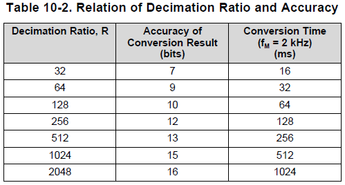
But the ADC0 is a 14-bit value(0~16383).

Is there any SD14 parameter setting wrong ?

Thanks.

====================================================================

void main()
{
WDTCTL = WDTPW + WDTHOLD; // Stop watchdog

// ROM RF13M module setup ** The following three lines are needed for proper RF stack operation
DS = 1; // ROM variable needs to be initialized here
asm ( " CALL #0x5CDA "); // Call ROM function ( Initialize function pointers)
asm ( " CALL #0x5CAC "); // Call ROM function ( Check part configuration)


initISO15693(CLEAR_BLOCK_LOCKS);
DeviceInit();

SD14CTL0 = SD14EN + VIRTGND;
SD14CTL1 = SD14UNI + SD14INTDLY0 + ADC0_CHANNEL;


while(1)
{

SD14CTL0 |= SD14SC;

__delay_cycles(1000000);

ADC_Value= SD14MEM0;


ADC_Volts = ((ADC_Value >> 8) *900)/(16383 >> 8);

//Enter Low Power mode
//__bis_SR_register(LPM3_bits + GIE);
}
}

====================================================================

  • Hello Allen,

    I am not following where you are getting the 32 bit idea from.

    The ADC result is stored in the first 14 bits of a 16 bit register. You can see this in the TRM, search for SD14RES and you will see the four result registers and the bits that the results occupy: http://www.ti.com/lit/ug/slau506/slau506.pdf

  • Hi Jacobi,

    Sorry, it caused your misunderstanding.

    I got the ADC0 value as below.

    The smallest difference seems is 32, not 1.

    I think the ADC0 is a 14-bit value(0~16383), so the minimum scale should be 1.

    No ADC0
    (Decimal)
    Difference
    1 5760
    2 5824 64
    3 5760 -64
    4 5728 -32
    5 5856 128
    6 5792 -64
    7 5696 -96
    8 5824 128
    9 5792 -32
    10 5696 -96

    Thanks.

  • Hello Allen,

    Okay now I understand. There is a relationship between the sample time and accuracy of the result. I think you are getting a 9-bit accurate result here, so with 5 bits not used for accuracy, you are seeing shifts of 32 bits for each result.

    To get higher accuracy requires long sample times.

    You can see the ratio of accuracy vs conversion time on Table 10-2 of the TRM: http://www.ti.com/lit/ug/slau506/slau506.pdf

  • Hi Jacobi,

    I can get 14-bit ADC accurate value after your suggestion.

    And use SD14IFG to check the ADC value is ready or not.

    But sometimes the ADC value looks weird.

    So I add 3 seconds delay between enable SD14 module and read ADC value.

    Is this delay necessary? How much time is correct?

    Thanks.

    =====================================================

    // Setup ADC 14-bit accuracy

    SD14CTL1 |= SD14RATE1 + SD14RATE2;

    =====================================================

    // Get the ADC0 value

    while(!(SD14CTL0 & SD14IFG)) {
    };
    delay_cycles_ms(3000);
    ADC0_Buffer[0] = SD14MEM0;

    =====================================================

  • Hello Allen,

    There should be no need for the delay. What is the input frequency of the signal you are measuring?

    Also I've seen a variant on what you are trying to do posted before, which if you are doing a single conversion maybe you can try out:

    while( !(SD14CTL0_H & ADC_SD14IFG_8BIT) );   // Wait for conversion to finish (for single conversion), ADC_SD14IFG_8BIT = 0x02

  • Hi Jacobi,

    I use a power supply to provide a stable voltage to the ADC.

    I can't find ADC_SD14IFG_8BIT in rf430frl152h.h.

    Is ADC_SD14IFG_8BIT the same as SD14IFG_H?

    By the way, could I increase the sampling frequency and reduce the conversion time?

    Thanks.

  • Hello Allen,

    Looking into it more, it seems maybe that was custom definition by someone else. So I think it could be SD14IFG_H. But knowing that now, I wouldn't recommend trying that instead.

    You wouldn't be increasing the frequency, but reducing the time samples are taken which lowers the accuracy. The frequency would be untouched, but the precision comes from sampling over time.

  • Hi Jacobi,

    1. So you means it should be work fine in below code (without any delay)

    while(!(SD14CTL0 & SD14IFG)) {
    };
    ADC0_Buffer[0] = SD14MEM0;

    2. So your recommendation is not to change the fm(2kHz) setting,

    because increasing the fm and reducing the conversion time will be cause reduced accuracy of ADC?

    By the way, may I know the maximum fm of ADC?

    Thanks.

  • Hi Allen,

    I'm going to ask another colleague to have a look into the issue with the sampling code.

    The Fm 2kHz setting is as fast as it will run, you would only reduce the speed if changing that.

  • Hello Allen,

    I read the tread but for me it is not exact clear how your code looks like. Can you please post the part of the code that troubles you. I will try to reproduce you problem.

    Best regards,

    Helfried   

  • Hi Helfried,

    Here is my code as below. It can get the ADC0 value and without any delay when read SD14MEM0.

    But I can't understand the value of the ADC is correct or not.

    In my understanding the ADC bit mapping table as below.

    ADC0 Min Max Mapping to Voltage (V)
    7-bit  0 127 0 ~ 0.9V
    9-bit 0 511 0 ~ 0.9V
    10-bit 0 1023 0 ~ 0.9V
    12-bit 0 4095 0 ~ 0.9V
    13-bit 0 8191 0 ~ 0.9V
    14-bit 0 16383 0 ~ 0.9V

    How should I shift the SD14MEM0 value to get the correct value?

    /* My Code  */

    void SetupSD14(u08_t channel)
    {
    SD14CTL1 = SD14UNI + SD14INTDLY0 + channel;
    SD14CTL1 |= (channel == THERMISTOR_ADC2_CHANNEL) ? SD14RBEN1 : SD14RBEN0;
    //SD14CTL1 |= (channel == ADC0_CHANNEL) ? (SD14RATE1 + SD14RATE0) : SD14RATE1; // 12-bit
    //SD14CTL1 |= (channel == ADC0_CHANNEL) ? (SD14RATE0) : SD14RATE1; // 9-bit
    //SD14CTL1 |= (channel == ADC0_CHANNEL) ? (SD14RATE0 + SD14RATE2) : SD14RATE1; // 15-bit
    SD14CTL1 |= (channel == ADC0_CHANNEL) ? (SD14RATE1) : SD14RATE1; // 10-bit

    SD14CTL0 = SD14EN + VIRTGND; // SD14 module enabled,
    SD14CTL0 |= SD14SC; // start the conversion
    }

    ...

    // Set and Read ADC0
    SetupSD14(ADC0_CHANNEL);
    while(!(SD14CTL0 & SD14IFG)) {
    };
    nfc_sys_data.ADC0_Buffer[0] = SD14MEM0;

    ...

    And the attachment is my captured ADC0 data.

    ADC0_Value_20191101.xlsx

    Thanks.

  • Hi Allen,

    I checked the values in your excel sheet and it looks ok for me. You asked how to shift the values to be correct, but you already did it.

    Just calculate the minimum step size : 0.9V / 2^14 and multiply that with your measured value. That's all. This is the same for all the filter settings. Only the precision of the measured value will change in dependence of the filter setting and the measurement time.

    Due to the structure of the CIC filter it does not mean that you will get at a decimation ration of 32 only 128 different values. But the precision is equal to 7 bit.

    Best regards,

    Helfried


  • Hi Helfried,

    So you mean the decimation ration of 32 is not only 128 different values. And the precision is equal to 7 bit.

    The precision means "SNQR" equal to "6.02 * 7 + 1.76 = 43.9", right?

    Thanks.

  • Hi Allen,

    the formula you used is for the ideal N-bit ADC. The correct one should be the Equation 5 in the TRM. I would go with the diagram in Figure 10-3 which shows the SNQR and corresponding precision.

    Best regards,

    Helfried

  • Hi Helfried,

    It is very helpful to me.

    Thanks for your help.