- Ask a related questionWhat is a related question?A related question is a question created from another question. When the related question is created, it will be automatically linked to the original question.
This thread has been locked.
If you have a related question, please click the "Ask a related question" button in the top right corner. The newly created question will be automatically linked to this question.
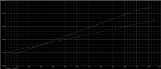
The OPAx387 model appears to be working, to a degree, but the outputs are above and below the rails, slightly. This occurs during the the bias calculation and during the DC sweep. I'm including pictures as a first step.
How is this possible?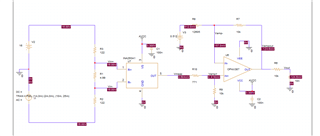
Hi Eric,
How is this possible?
There is an issue with your 512mV applied at the inverting input on the OPA387's circuit.
As it is configured, you solve the Vout using superposition method.
1. Consider the output of INA293 is 0V, or ground Vin voltage source as simulated, then Vout1 = -512mV * (10k/12.605k) = -0.40619V
2. If you ground V1 or 512mV, the Vout2 = 0V
3. combine Vout = Vout1 + Vout2 = -406.2mV
The Tina-TI simulated at approx. -127.26mV, because it can not go lower than the figure or GND.
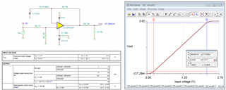
If I placed -0.5V at the V- rail, then the circuit's output simulates at -406.04mV, which it agrees with hand calculation.
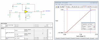
If you configure V1 = GND, then output is in a linear relationship with Vin, which is run from 0V to 1.9V, and the gain of the circuit is approx 3.16V/1.9V = 1.8947 V/V
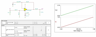
OPA387 for PSpice 02222022.TSC
If you have additional questions, please let us know.
Best,
Raymond
Thank you for the detailed reply! The purpose of the circuit is to introduce a negative offset in the output voltage as well as add gain, to condition the signal for an A/D. In addition, I'm trying to do this with a single supply. The circuit is based on the "Non-inverting op amp with inverting positive reference voltage circuit" in the TI Analog Engineer's Handbook. It seems that "in real life" the circuit will work fine, perhaps the excursions past the rails are clamped in actual operation. However, I still need to get an accurate simulation - especially since this circuit seems to push the limits of the math used to model its operation! I'm also struggling with convergence problems, but was able (just once!) to get the transfer function I expected, before the simulation returned to being unable to converge. The nondeterminate behavior is irksome - as is my inexperience with the intricacies of getting around SPICE's limitations. Do you reccomment TINA over PSPICE-FOR-TI for this work?
Hi Eric,
"Non-inverting op amp with inverting positive reference voltage circuit" in the TI Analog Engineer's Handbook.
Are you referring to this circuit, except the calculator is shown a buffer configuration with Noninverting Level shift.
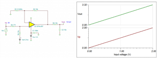
You probably has the following calculato. In case that you don't, you may down it from the link below.
https://www.ti.com/tool/ANALOG-ENGINEER-CALC
The circuit gain is G = (1 + R2/R3) = 1.7933 V/V. Apply the superposition method:
If we Ground Vin, Vout1 = G*(R5/(R5+R4)*Vref) = 1.7933*(771/10771)*(-21mV) = -2.6957 mV
If we Ground Vref, Vout2 = G*(R4/(R4+R5)*Vin = 1.7933*(10000/10771)*Vin = 1.6649*Vin
So Vout_tottal = Vout1 + Vout2 = 1.6649*Vin - 2.6957mV, which is the transfer function.
If Vin = 0V, then Vout_total = -2.6957 mV,, If the circuit has additional Vos, then the Vout should be compensated to near 0mV, as shown in the image below (without violating Vcm requirements for a single supply rail).
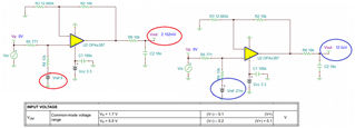
OPA387 Level Shift 02232022.TSC
If you have additional questions, please let us know.
Best,
Raymond
Yes it's the circuit from the Analog Engineer's Cookbook that you mentioned (p.146 current version, see attached screenshot.). However, I don't understand your analysis of it, since removing the positive inverting reference changes its function. Life would be easier if indeed I had access to a negative supply to add to the input signal - at a minimum I could understand what's going on better simulation-wise! However, the board I'm designing is a Raspberry PI Hat, and real estate is at a premium so adding another power supply along with filtration to meet ripple requirements would be my last choice! I'm already using high-integration analog components (thanks, TI!) to save space.
What's interesting is that the authors give an example without discussing what you have brought up here, or the issues with simulating the circuit as I have found. Their math is based on the + and - inputs to the op-amp being at the same potential, so probably what's missing is a discussion about what happens near the limits of the circuit's outputs. My desired transfer function is Vo = 1.66Vi - 0.4062. I did manage to get the circuit I gave you to simulate last night and it comes close to this transfer function, except at the limits, which is OK.
The end application for this schematic is accurate 12-bit ADC analysis of a 4-20ma current loop while providing high common-mode and ESD immunity (I haven't added the TVSs to the circuit yet!). More obvious isolated solutions take up too much real estate and are out of budget. And many of the design approaches I considered are impossible because of the current parts shortage. 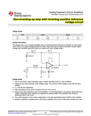
By the way, I'm using Windows 11 and TINA doesn't seem to start on it. So I'm continuing to use PSPICE-FOR-TI. Can you point to any good documentation on reducing problems calculating the bias point? That's where I'm stuck right now: PSPICE fails to converge on voltages near the OPA387.
Hi Eric,
Let me get it back to you, since the simulated voltage should not go below the ground with the single supply rail or V- = GND.
My desired transfer function is Vo = 1.66Vi - 0.4062...
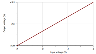
Since Vo can not go below ground, the transfer function will work when Vin > 0.2447V. If you provide me the Vout operating range, I will see if there is a way to get around. If Vin is required to be 0 <= Vin < 2.2V, you will need a negative supply rail.
In the SBOA262A app note, 2 < Vin < 5 is the operating range, and it does not work below 2V in Vi.
By the way, I'm using Windows 11 and TINA doesn't seem to start on it.
I do not know that the Tina-TI (ver. 9.3.2) does not work in Windows 11 OS. Sorry, I am unable to help in the issue. I am using Windows 7 and Windows 10 with Tina-TI.
Can you point to any good documentation on reducing problems calculating the bias point?
We have series of Op Amp Video Training clips, but it takes time to go through it, see the link below.
Regarding to negative voltage regulator. You may consider our LM27761, LM2776, LM2662, LM7705 negative bias voltage generators, which a switched capacitor voltage inverter. If you input a positive supply voltage, it will generate a negative voltage rail. If you do not have much PCB remaining on a board, then these options may not be useful for the design.
Please let me know if I can assist you other issues. If OPA387 pspice model has issues, I will ask engineer to fix it.
Best,
Raymond
Hi Eric,
I was using the one year old Macro model instead of the latest one. Anyway, with the latest pspice model, Vout does not go below the GND (-1.8mV) in a single supply voltage rail. However, your input or linear region can only be between 0.511V to 4.677V. The pspice model is dated on 9/21/2021. Please make sure that you are using the latest model that has the same date approximately.
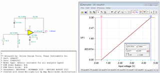
Please balance the input resistance and you will get a better range If you have additional questions, please let me know.
Best,
Raymond
Hi Eric,
Sorry, I forgot that you'd like have a transfer function: Vo = 1.66Vi - 0.4062
Below is the circuit, but you input range is limited.
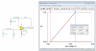
If you have other questions, please let me know.
Best,
Raymond
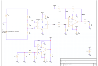 Yes, this is what I'm shooting for. I have started to look at the switched-cap voltage sources but they will need further regulation to remove ripple... in other words more components on my precious board real-estate! There are two problems with this circuit: PSPICE doesn't like it when I add the second x387 for the low-impedance voltage source: bias conditions are not converging; and second, I am not certain what happens if Vi goes below 340mv. Ideally the x387 just puts out zero volts; worst case the device is damaged. I'm using these "nonlinear" regions at the top and bottom as a way to place the A/D in a range that signifies "too low" or "too high" error conditions on the 4-20mA current loop. In other words the "real" desired transfer function is Vo = MIN(MAX(1.66Vi - 0.406), 0), 3.3)
(By the way I'm familiar with TI's 4-20ma receiver chip but as a DIP, it's far too large to fit on my project.)
I will take the video lab instruction you suggested today. I wish there was one that was about "How to fix PSPICE convergence problems"! You will laugh at this but I first used SPICE in 1980 - using punched cards!
Please note that the attached schematic is the one I can't get to converge on bias conditions: adding the second x387 seems to prevent convergence, even though the voltages that aren't converging are all on the pins of the x387 used as the amp/level shifter.
Hi Eric,
I have started to look at the switched-cap voltage sources but they will need further regulation to remove ripple...
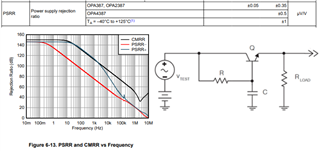
Yes, it will introduce some ripple noise over existing circuit. Please use low ESR capacitors to bypass the noise to ground. Our boost charge pumps LDOs should work good for the op amp application (high PSRR in OPA387). Normally, RC LPF should work good enough.
If you want to further attenuate the switching noises, you may use the capacitor multiplier method to further reduce ripple noises, see the attached image below (this is for positive noisy voltage source and you want to implement one for negative supply).
How to fix PSPICE convergence problems...
I had the same issues when I am dealing with PSPICE-FOR-TI, especially when more components are involved. Tina-TI is much more user friendly in this regard.
BTW, the precision op amp training videos are excellent, but it may not get what you are looking for right away, especially you know a lot about the design. You may try to skip certain frames and accelerate through the contents.
If you have additional questions, please let me know.
Best,
Raymond
Thanks for the heads-up on TINA over PSPICE. I found a virtual Windows 10 machine and installed it. However, neither part that I'm using (INA290/293) nor the OPAx387 are in its library. I found library elements on the device pages. Can you advise on how to install them?
I just pointed TINA to the models in my download folder and created my circuit, I including a precision source and another x387 as the low impedance reference driver. The whole circuit is working as I expected! The difference in computation time (and the fact that I actually got a result) is amazing. It looks like PSPICE-FOR-TI needs more work :(
Hi Eric,
INA293/INA290 models are found in the link below. You may download them directly.
Please note that there are many different models or choices. For Tina-TI, you need to pick TINA-TI REFERENCE DESIGN (ready to run simulation). PSpice Model is typical referring to a product in compatible PSpice library.
Typically, for search OPA387,
1. please enter OPA387 datasheet over google search engine.
2. Under Ti.com, you will find the following circled categories and click on each in sequence and you will find PSpice Models and reference design are allocated.
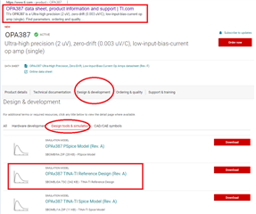
https://www.ti.com/product/OPA387#design-tools-simulation
In addition, you will find the Tina-TI training in the following link. It will save you a lot of frustration from learning a new simulation tool.
https://training.ti.com/introduction-tina-titm-simulator?context=1127691-951878
If you have additional questions, please let us know.
Best,
Raymond
Well with TINA, I think I have the best implementation of the solution with these devices. But... I'm still concerned about the negative common mode specification of the INA190, which is far less than I'd like. I've been looking at instrument amplifier solutions that could have a more balanced and wider common mode input maximum so that I can increase the reliability of the circuit in the unfriendly production process environments. Do you have any suggestions on products or approaches that TI might be able to recommend?
Hi Eric,
Below is the instrumentation amplifier (IA) selection.
If you are able to provide me with gains of IA, input Vcm and Vout range, I can simulate one for you later. INA826 is a low cost IA, but we do have tons of options. Please see the selection below.
Best,
Raymond
Here’s what I’m trying to achieve:
Build an accurate 4-20ma current monitor Analog Front End for a 12-bit A/D that uses minimal board space and parts cost to achieve performance required for process control in electrically challenging environments at overall low cost (such as interfacing with the Raspberry Pi running REXYGEN control software)
1) Deal with common mode voltages that might occur with a 20ma loop that was not referenced to a common ground with the interface, without expensive full galvanic isolation. This means dealing with ground loops or accidental connection to 120V AC as well as EMI, ESD, and reverse connections or incorrect power supply connections. For this I’d like a common mode specification of over 120V with some safety margin that allows for use of TVS devices to prevent damage to the interface. However, based on my research so far, it seems that 60V might be more doable, and I can live with that.
2) Use 80% of the 3.3v, 12-bit A/D FSR (the remaining 20 percent for detecting over-and-under current conditions). This means overall error has to be in the neighborhood of .05% if possible on budget. Oversampling to get more bits of A/D range seems futile but it could be useful to reduce the effects of noise in the signal. So the Vout range should be 0-3.3v, minus any necessary amounts to match limitations in the devices.
3) The gain of the IA should be able to accommodate an input range appropriate for a shunt resistor operating on 0-20ma and produce the required Vout either alone or with an additional op-amp stage that also level-shifts to remove most of the 0-4ma range in the measured output since it’s a “waste” of the A/D FSR. The circuit you and I worked on used roughly 2.8ma-21.6ma with clipping to set the FSR range, using the extra 10% on either side as an under/over current signal and to ensure linearity. Based on EIA standards, the shunt resistor should be 250 ohms, but in my design I used a 5 ohm resistor as the shunt and added 2x122 ohms to bring the overall shunt to EIA standards. I’m also OK with going to 500 ohms total since this makes selecting a TVS easier.
4) I have a strong preference for single-supply 3.3v (cost/real-estate) but I know that the instrument and difference amps get better Vcm-max when they are fed a balanced supply, so I’m willing to consider that (I can use at least one +16v supply as the sources for the current loop which my customers would appreciate.)
Thank you again for your help!
Eric
Eric,
Enclosed is our 4-20mA 2-wire transmitter with XTR117. XTR111 is our 3-wire 4-20mA transmitter. Of course, there are other. Or you make your own 4-20mA current loop with a precision op amp.
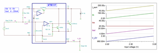
We can adapt one of the IC and convert the 4-20mA signals, see the attached simulation.
XTR117 0-5V 4-20mA 02262022.TSC
Regarding to you input, I am not certain what you wanted. You have 16Vdc and 5mV AC is riding on top of it. What is the frequency?
I am sending over the file and please make any changes and send it back to me in Tina. Then I will put all these together. The sensing current is a bit low.
INA826 CURRENT SENING 02262022.TSC
Best,
Raymond
Hi Raymond,
I examined the circuits you proposed. I don't understand the first one with the XTR117, since it's a transmitter chip and I'm trying to build a receiver. Did you intend the input voltage to your circuit to come from the voltage across the shunt resistor for the 4-20ma receiver, and the A/D would sample the voltage across Rload?? If so, I don't understand why this circuit would be better than the one I developed in meeting the project requirements, since there is additional error from having two load resistors and considerably more current is consumed, as well as board space.
The second circuit seems to be oriented towards an AC input signal on top of a CM DC signal, which is not my application. My application is very low frequency and full-scale, resulting from a measurement sensor like tank level or humidity, etc. So my focus is accuracy in measuring the 4-20ma range of essentially a DC input, with a little overrun capability to sense a fault condition. The reason I am concerned about CM input is first that in the event of high-side measurement, the loop power supply is the CM voltage. And, there are issues with EMI and ground loops that can produce CM signals so the circuit needs both high CMRR and survivability of CM excursions (with appropriate TVS protection.)
Essentially, the circuit I originally showed you (which simulates correctly now on TINA) would be perfect, except for the asymmetric Vcm-max limitation of the INAx290 (I used the 387 originally since Pspice didn't come with a model for the 290).
Hi Eric,
Did you intend the input voltage to your circuit to come from the voltage across the shunt resistor for the 4-20ma receiver,..
Maybe it was my misunderstanding. I recalled that you mentioned a DIP package of 4-20mA receiver (likely RCV420). Then you may require 4-20mA transmitter to communicate via the current loop, and that is why I thought of XTR117 or XTR111 to minimize the space issue. If it does not apply, please ignore my suggestion.
So my focus is accuracy in measuring the 4-20ma range of essentially a DC input, with a little overrun capability to sense a fault condition...
If you are talking about replacing INA290 I-to-V converter with an instrumentation amplifier (IA) + wide range of common mode input voltage, we do not have direct placement to handle the current sensing application.
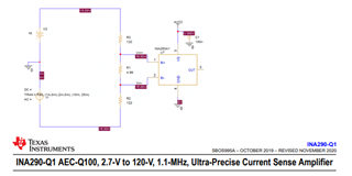
You may have to use INA148 or INA149 or INA159 other difference amplifiers to lower Vcm in order to work with IAs.
If you have additional questions, please let me know.
Best,
Raymond
Thank you. I'll try designing with the INA149. I'm crossing my fingers that either TINA or Spice will support modeling the dual-rail power supply converter I need as well! Overall I expect a lot more board space to be used, but I hope that when my layout artist gets to work, it will still fit.
Hi Eric,
Enclosed is INA149 Linear Operation Check in Tina.
INA149 Linear Operation Checker.TSC
It should be identical to the INA149's datasheet, but it is a bit easier to check input Vcm with help of Tina for a linear operation, if you are using supply rails that are different from the datasheet.
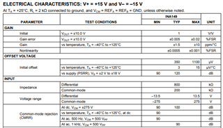
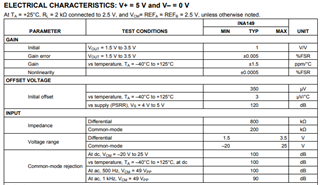
If you have additional questions, please let us know.
Best,
Raymond
Thank you. Speaking of supply rails.... presuming I can find any TPS65130/1 parts, how do I simulate them? Webench doesn't create the whole circuit, yet it recommends simulating the circuit to be certain it works. And there doesn't appear to be a model for TINA, or a model in PSPICE :(
Hi Eric,
I do not know why we do not have pspice model in these (the product is supported by CPP-CPP team over E2E). However, we do have TPS65130EVM-839. You may request sample for it, but it may take time.
I do not have good suggestion for you.
Best,
Raymond
I will post in that forum about the model. Waiting for an evaluation module when I'm not sure this strategy will fit on my board is probably not the best approach. However, the INA149 circuit simulates well, is linear at a variety of loop power supply voltages up to 40v, meets my accuracy needs up to Vcm of 36v which is good, and after tweaking the burden resistor to be larger, has sufficient dynamic range and noise specs to work well for me. OK, I didn't get that much sleep calculating the SNR LOL! My remaining challenge with this circuit is figuring out input protection against ESD since the input resistors have to be a low value. 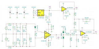
Hi Eric,
Ok, take it easy.
INA149's input and output protection is very high. Please let us know if this is not enough for the application.

Best,
Raymond
Yes, it is high which is great because it makes the remaining work to meet ESD standards easier. However my understanding is that the standard IEC 1000v discharge will destroy it, so I have to add additional TVS (modeled by voltage controlled switches in my schematic). The 500v protection solves problems with ground loops as well (which is the major reason I'm picking a high Vcm part since I have to get all that done in minimum board space which isn't possible with full isolation.)
Hi Eric,
If you want higher ESD protection at the input, you may consider to implement low leakage bidirectional TVS at the INA149's input or add additional current steering diodes at the input to absorb any possible ESD voltage spikes and energy.
I noticed that you have current steering diode protection at the output at 3.3V (AVCC3.3) as well. I do not know what type of transient overvoltage that the application is required to be protect. Anyway, the protection will work better if you place a zener or TVS at the 3.3V supply raill. When the current steering diodes are turned on momentarily due to overvoltage transient, the excessive current is able to steer to ground and protect 3.3V supply rail or IC. Without the TVS or Zener clamp at AVCC3.3 rail, if transient current can not find a path to ground, may do some damage if transient current is unable to find a path.
(BTW, these current steering diodes and TVS shall have faster response time than ESD diodes reside inside of INA149 IC and lower ON voltage threshold).
The image below is captured from a different application and 24V zener is applicable for that application and supply rail. I am presenting it here as an example.
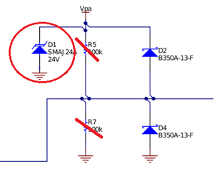
If you have additional questions, please let us know.
Best.
Raymond
Hi Raymond,
The Schottky diodes at the output of the INA149 are there to convert the bipolar +/-15v possible output of the INA149 into a unipolar 0-3.3v input for the opamp. I scaled the burden resistor to match the 0-20ma expected currents, with a little extra room for overcurrent detection, but if for example 40ma was put through the resistor, the INA149 would put out a voltage that could damage the opamp. I know, I need to move the diodes closer to the opamp to prevent damage to the INA149 output stage, just need to do a simulation to see how it affects the frequency response.
Your idea of the TVS on the supply rail is good but may not be necessary as the Schottky diodes are not for transient protection. If they end up being involved in a transient, I expect the INA149 will already be toast!
Hi Eric,
The INA149's input and output terminals are equipped with ESD protections, see the previous absolute max. ratings. In an event that the internal ESD diodes start to conduct current, the diodes' current must be limited to +/-10mA without damages. INA149's input should be well protected, especially if you are going to place addition surge protections at its input.
The internal ESD diodes (schottky) is able to absorb a limited amount of energy or dissipation without damage. As the ESD ratings indicated, it is in compliance with a typical ESD ratings (may not be the latest higher ESD ratings, but it was the standard back 10 years ago.).
If the INA149 is using +/-15Vdc rails and INA149's output is going up to 3.3Vdc or so, the output ESD diodes should not be conducting in normal case. So the ESD internal diodes at the INA149's output should not be conducting. So I think that INA149 will be ok for the application.
If there are any unexpected transient surge occurred at the output of INA149, OPA387 may exhibit higher stress conditions than INA149, and may get damaged first.

When selecting the external schottky diodes for external transient protection, you may consider low junction capacitance and low conducting voltage schottky diodes. As you stated, the regular ones may not be fast enough to respond to a transient events.
If you have additional questions, please let us know.
Best,
Raymond