Hi Team,
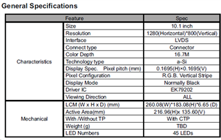
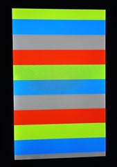
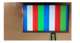
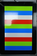
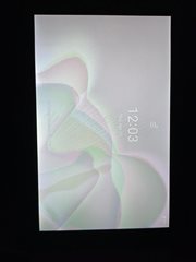
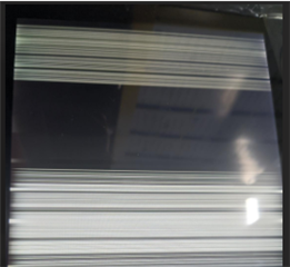
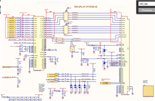
we are integrating 10.1 inch display with IMX8MM custom board through MIPI-LVDS bridge as shown below.
LVDS display Integration:
- Schematic diagram
Dtsi changes
&i2c4{
clock-frequency = <300000>;
pinctrl-names = "default";
pinctrl-0 = <&pinctrl_i2c4>;
status = "okay";
...
...
lvds_bridge: sn65dsi83@2c {
compatible = "ti,sn65dsi83";
reg = <0x2c>;
ti,dsi-lanes = <4>;
ti,lvds-format = <2>;
ti,lvds-bpp = <24>;
ti,lvds-channels = <1>;
ti,width-mm = <149>;
ti,height-mm = <93>;
enable-gpios = <&gpio2 9 GPIO_ACTIVE_HIGH>;
interrupt-parent = <&gpio2>;
interrupts = <8 IRQ_TYPE_LEVEL_HIGH>;
pinctrl-names = "default";
pinctrl-0 = <&pinctrl_dsi_lvds_bridge>;
status = "okay";
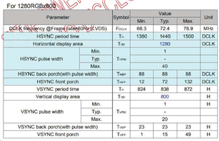
display-timings {
lvds {
clock-frequency = <72400000>;
hactive = <1280>;
vactive = <800>;
hback-porch = <88>;
hfront-porch = <72>;
vback-porch = <23>;
vfront-porch = <15>;
hsync-len = <80>;
vsync-len = <10>;
};
};
port {
sn65dsi83_in: endpoint {
remote-endpoint = <&dsim_to_sn65dsi8>;
};
};
};
};
&lcdif {
/*trusty;*/
status = "okay";
};
&mipi_dsi {
status = "okay";
port@2 {
dsim_to_sn65dsi8: endpoint {
remote-endpoint = <&sn65dsi83_in>;
attach-bridge;
};
};
};
&iomuxc {
pinctrl_dsi_lvds_bridge: lvds_bridge_gpio {
fsl,pins = <
MX8MM_IOMUXC_SD1_DATA7_GPIO2_IO9 0x16
MX8MM_IOMUXC_SD1_DATA6_GPIO2_IO8 0x19
>;
};
- Added below drivers in source code
drivers/gpu/drm/bridge/sn65dsi83/
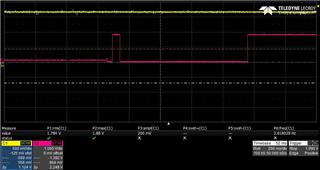
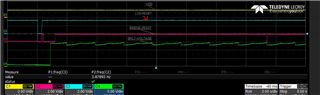
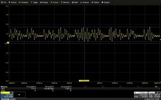
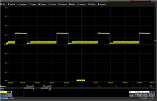
- After flashing, we have observed that driver is failed to reset the bridge and below are the logs for the evidence
sn65dsi83 3-002c: sn65dsi83_probe
[ 2.604061] sn65dsi83 3-002c: failed to parse enable panel gpio
[ 2.610051] sn65dsi83 3-002c: sn65dsi83_brg_power_off
[ 2.634134] sn65dsi83 3-002c: sn65dsi83_brg_power_on
[ 2.650154] sn65dsi83 3-002c: sn65dsi83_read client 0x(____ptrval____)
[ 2.657291] sn65dsi83 3-002c: (efault) failed reading at 0x3e4c752e
[ 2.663574] sn65dsi83 3-002c: sn65dsi83_brg_reset ret=-6
[ 2.674739] sn65dsi83 3-002c: Failed to reset the device
[ 2.680060] sn65dsi83 3-002c: sn65dsi83_probe, ret=-19
[ 2.685729] sn65dsi83 3-002c: Failed to reset the device
[ 2.691167] i2c i2c-3: IMX I2C adapter registered
and on adb shell, with command $ i2cdetect -y 3, I couldn’t see the lvds display registration.
Could you please help us how can we reset the lvds bridge.
Are we missing any configuration in LVDS bridge integration?
Thanks,
Raghavendra