This thread has been locked.

If you have a related question, please click the "Ask a related question" button in the top right corner. The newly created question will be automatically linked to this question.

UCC28950: UCC28950 no phase shift

Part Number: UCC28950

Tool/software:

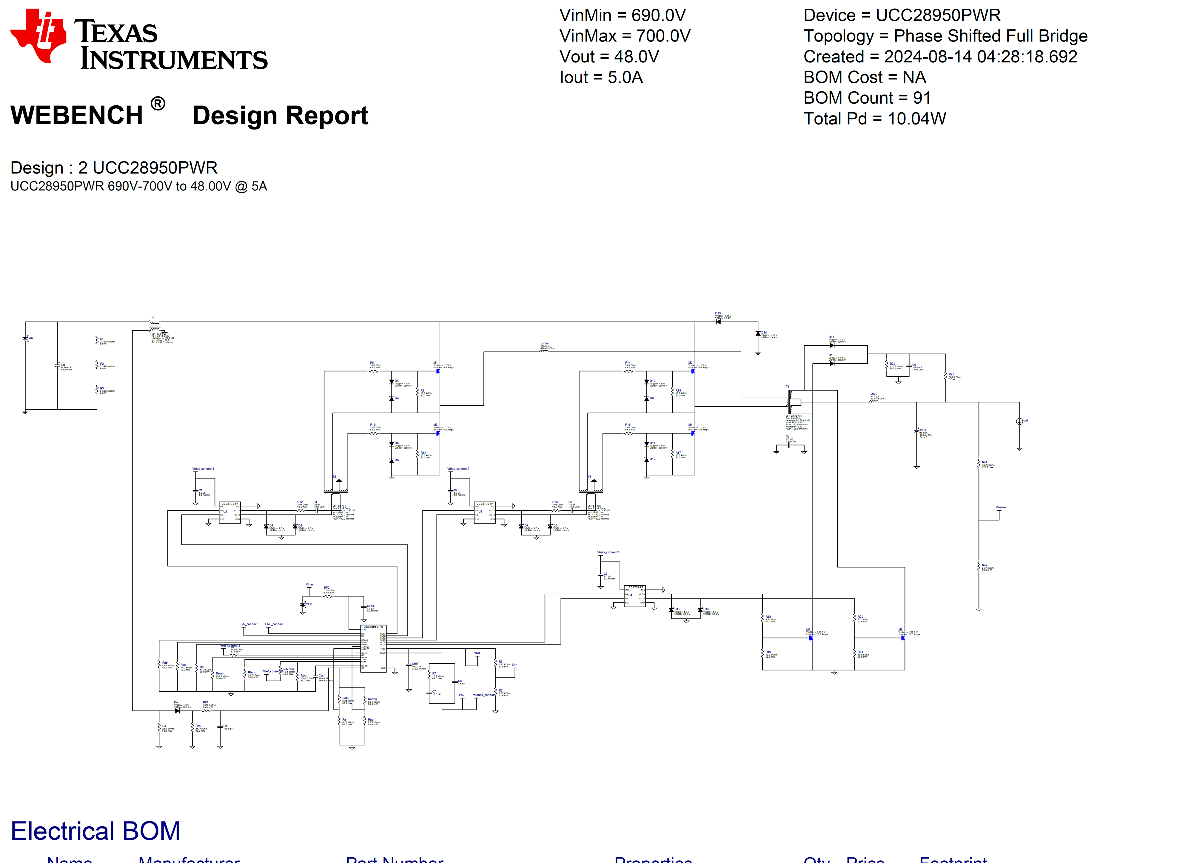
Currently, we are facing a problem with the PSFB design based on UCC28950. The design is 240W, 48Vout, 5A Iout, 700Vin, Fsw 100KHz. In addition, the Tx turn ratio is 12.4:1.  I use UCC27324DGNR as gate driver (I highlight here because I published a question before and I cannot reply a wrong answer. So I re-publish this question) to provide two half bridge Vgs (High side is not refer to GND). 

--------Q1------Q3          Q5---------|--Vout+

           |            |   TX     -------L---|---Vout-

--------Q2------Q4          Q6---------|

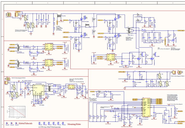
If the Sch is blurry, please refer to the EVM design, which is https://www.ti.com/lit/an/slua560d/slua560d.pdf?ts=1738633435221&ref_url=https%253A%252F%252Fwww.google.com%252F

The problem is, in the light load situation, we can get 48Vout. But there is no phase shift for the Vds (Q3, and Q4), so there is no deadband on the Tx waveform. Ideally, when I give 700Vin, based on the turn ratio of the Tx, I can get 53V without control. If I get 48V, the TX waveform should have a deadband, but it is not. After that, I add load, the Vout starts to drop.

So, can you please help us, with why there is no phase shift?  

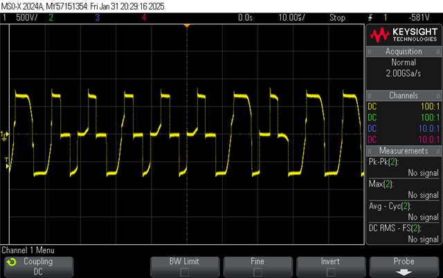
Please see the waveform attached.

The picture below is the Tx waveform, which is damping when the load is only 200mA. When the load is above 200mA, the waveform will become an “H-bridge” with 50% duty cycle.

The picture below is the Vds of Q1 and Q4. Yellow is Q1, Green is Q4. This is still on the 200mA load situation. You see the phase shift angle (direction) of Q4 is wrong.


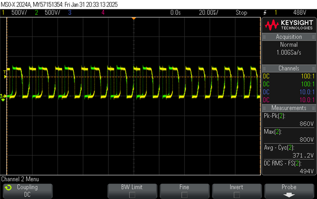
I am very confused why no phase shift (or the wrong phase shift happening). Is that because of Tx or IC set up? Or Tx turn ratio not correct.

  • Hello,

    The following thread gave recommendations on the issue you are having.

    https://e2e.ti.com/support/tools/simulation-hardware-system-design-tools-group/sim-hw-system-design/f/simulation-hardware-system-design-tools-forum/1469291/ucc28950-the-psfb-design-based-on-ucc28950-has-no-phase-shift

    Your schematic was hard to read.  Could you sent a clearer one so I can double check it?

    If you do not have phase shifting the controller is at 100% duty cycle.  This could indicate that your transformer turns ratio is off or your feedback loop is in error.

    The following link will bring you to an application note covers how to proerly select/check the transformer turns ratio.  There is also a schematic that shows how to properly setup the feedback loop.

    https://www.ti.com/lit/pdf/slua560

    Regards,

  • Hi Mike, I have created a link below, using that you shall be able to access schematic, calculation and transformer data.

    https://we.tl/t-92enVGueLr

  • Hi Mike,

    While looking in to https://www.ti.com/lit/pdf/slua560, and the UCC28950 spreadsheet calculator SLUC222D, the calculations for ADEL and ADELEF are done based on considering Vref, whereas the webench simulation we did (can be found in below link) shows ADEL and ADELEF connected to CS pin via resistor network. Our design follows the Webench, could you please guide how do we calculate resistor values for ADEL and ADELEF if they are connected to CS pin.

    https://we.tl/t-n2jFkkSaN5

  • Hello,


    Your inquiry has been received and is under review.


    Regards,

  • Hello,


    The application note SLUA560 uses a fixed delay approach which is a fixed voltage at ADEL and ADELEF.  This can be done with a resistor divider from VREF as shown in application note SLUA560 or tying ADEL and ADELEF to ground.

    If you want to use the adaptive delay approach by using resistor dividers from the CS pin to ADEL and ADELEF this technique is used when trying to eliminate the body diode conduction on the primary.  This mostly a trial an error process that most engineers struggle with.  To save time I would use the fixed delay approach that is discussed in SLUA560.  This is a popular approach to PSFB design and are customer have great success accomplishing this.

    If you wish to try adaptive delay which is a trial an error approach.  I would suggest starting with the fixed delay approach to make sure you have the design running and are achieving ZVS.  Once you have the designing running then you need to study the CS signal, switch nodes, and SRs signals at 25, 50, 75 and 100% load to see if an adaptive delay would provide you any efficiency benefit.  You would then have to study figures 6-2, 6-3, 6-5 and 6-6 and select the curve that best fits your application.

    I would recommend using the fixed delay approach described in SLUA560.  It will save you many hours in the design and troubleshooting process. 

    Thank you for interest in Texas Instruments (TI) products.  If you have a related question, please click the "Ask a related question" button in the top right corner. The newly created question will be automatically linked to this question.

    Regards,