This thread has been locked.

If you have a related question, please click the "Ask a related question" button in the top right corner. The newly created question will be automatically linked to this question.

TPS40210 SEPIC Gain/Phase simulation using TINA-TI

Other Parts Discussed in Thread: TPS40210, TINA-TI, TPS40210-Q1

Hello,


I want to simulate Gain/Phase of TPS40210 SEPIC configuration.

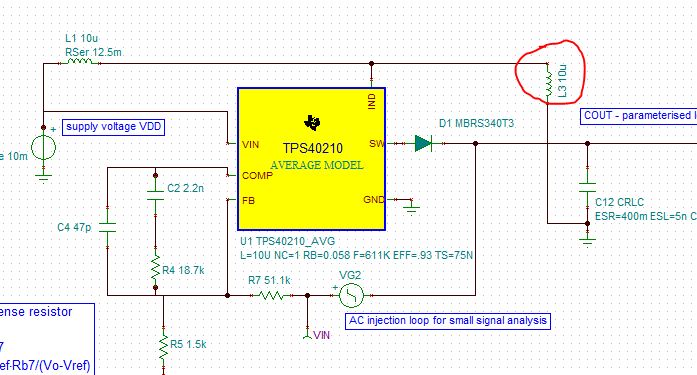
TPS40210 product page has “TPS40210 TINA-TI Average Reference Design (Rev. C)” and it is example of BOOST converter.


Please advise if I can simulate Gain/Phase of SEPIC configuration when I modify boost circuit as follows.


If yes, please advise how to program following macro parameter of TPS40210.


Best Regards.

  • Hello,
    Please answer my question.
    Best Regards.
  • Ushikubo-san,

    I have not used the average model for a Sepic configuration. The parameters that are passed to the subcirucit are:

        L: PRIMARY INDUCTANCE IN HENRIES
        NC: CURRENT TRANSFORMER TURNS RATIO: used to calculate the peak inductor current
        F: SWITCHING FREQUENCY IN HZ
        EFF: EFFICIENCY: used to calculate equations of input and output currents of the boost controller.
        RB: CURRENT TRANSFORMER BURDEN RESISTOR IN OHMS: Rsense * internal gain (10m*5.8).
        In your case, check what the current sense resistor used in the application and use the value of that * 5.8
        TS: PROPAGATION DELAY TIME IN THE CURRENT LOOP - used to calculate the peak inductor current
        in the boost subckt of the model.

    You will need to change the inductance value based on your inductor change (In your case, 33u * 2 = 66u). You may need to update the switching frequency and efficiency as well, but that would depend on your design changes.

    I would connect your second inductor from the IND pin to the ground for your Cout, not from the diode on the SW pin.

    Here is an example from the reference design:

    You may also want to refer to the following document. It has some very good information about Sepic designs.

    Sepic Analysis.pdf

  • Hello Britt-san,

    I tried to make simulation circuit of PMP4608 boost reference design to do gain phase simulation.

    I made attached TINA-TI circuit refer to Figure4 of Sepic Analysis.pdf.

    TPS40210_Sepic_PMP4608.TSC

    I did gain phase simulation and result is follows.

    Following is Gain and Phase result of PMP4608 Test Report and curve is different with my TINA-TI.

    Please check my TINA-TI file and correct my mistake.


    Best Regards.

  • Hi Toshio San

    We are currently trying to run the boost average model in the SEPIC configuration and see what you are seeing in the TINA-TI simulation as well. However, the engineer who is the correct person to comment on whether you can use this AC linearized model for the boost configuration in the SEPIC is on leave. We will follow-up with you after July 4th.

  • Hello Ranjanir-san,


    Thank you for your reply.


    SEPIC simulation is request form TPS40210-Q1 customer, so please answer my question when correct person return to work.


    Best Regards.

  • Ushikubo-san,

    If you remove the reference to the Vout GND and replace it with a GND connection, the simulation looks much more like the measured data. I am trying to determine what effect the additional components would have on the frequency response using the Average model right now, but I thought I would update you first. If I find out that the additional components are necessary for modeling, I will let you know. Here is the .TSC file I used:

    3426.TPS40210_Sepic_PMP4608.TSC

    Please let me know if you have any additional questions. I apologize for the delay as I was out of the office for a couple of weeks.

  • Hello Britt-san,


    Thank you for your answer.


    I tried your file and result was close to measured result.

    But your file doesn’t include C28, R102, C15, C100 and C101.


    Please confirm the necessity of these components in simulation circuit and let me known.

    Best Regards.

  • Ushikubo-san,

    I have discussed this with one of our product experts. He believes that the additional components will affect the Bode plot of the design, however, their purpose is to supply the current necessary for the second coil of the SEPIC design. In the case of the PSpice model, the current supplied is set by the internal block and the parameters passed to it, so I do not believe that the extra components are necessary as their function is "modeled" in the average model of the device. This MAY NOT always be the case, but for this particular example using the TPS40210, I believe that the additional parts are NOT necessary for the Bode Plot simulation only.

    I believe that this is why the measured data is similar to the simulated data here as well. Please remember that the model was not characterized for a SEPIC topology, but it appears to be similar in its behavior with simply adding the additional coil.

    So, with a bunch of assumptions, I think that the file I provided is similar to how the overall board would behave for a simple Bode Plot. As always, you must verify the performance of any board with measured data before defining the design as sufficient.

  • Hello Britt-san,


    Please answer additional following question about TPS40210 macro parameter and use case of Coupled Inductor.


    L: PRIMARY INDUCTANCE IN HENRIES

    Q1: Shall I use 44uH(22uH * 2) or 22uH when L1=22uH and L2=22uH?


    NC: CURRENT TRANSFORMER TURNS RATIO: used to calculate the peak inductor current

    Q2: Please explain the meaning of NC and how to obtain this value.


    TS: PROPAGATION DELAY TIME IN THE CURRENT LOOP

           - used to calculate the peak inductor current in the boost subckt of the model.

    Q3: Original TINA reference design use 75ns.

           Is this from Lead edge blanking time of datasheet?


    Q4:

    Please advise how to set the value of L1 and L2 in case of using Coupled Inductor like PMP8656.

    PMP8656 use 10uH Coupled Inductor, shall I use 20uH(10uH * 2) for L1 and L2?

    PMp8656_回路図_sluraj5.pdf

    msd1583.pdf


    Best Regards.

  • Ushikubo-san,

    For the example I provided, I would use 44uH for L, NC=1, RB=0.029, EFF=0.9, and TS=75N. TS is NOT the leading edge blanking time, it is an estimate of the delay in the amplifier loop of the TPS40210, including the compensation network. The 75N should be good for most TPS40210 applications. Please remember that the average model was NOT developed for SEPIC applications and may give results that do not align with measured data. The example I showed did give reasonable results for a SEPIC design with a LOT of assumptions.

    I do not know if the model can be used for all SEPIC configurations and would hesitate to recommend it for general usage for all SEPIC designs. The coupled inductors may provide a different issue as to how the schematic should look for the average model. I have not used any of our average models for this kind of design.