This thread has been locked.

If you have a related question, please click the "Ask a related question" button in the top right corner. The newly created question will be automatically linked to this question.

WEBENCH® Tools/LM25118: LM25118 – About same circuit for multiple output

Part Number: LM25118

Tool/software: WEBENCH® Design Tools

Hi,

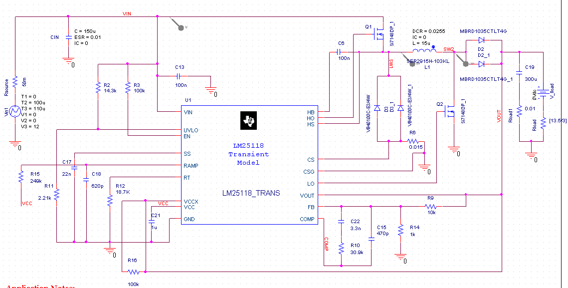
I would like to use LM25118 at the following condition.

[Use condition]

Vin=10.8V to 15V

Vout is changed from 6.0V to 15V.

Iout=3.0A (max)

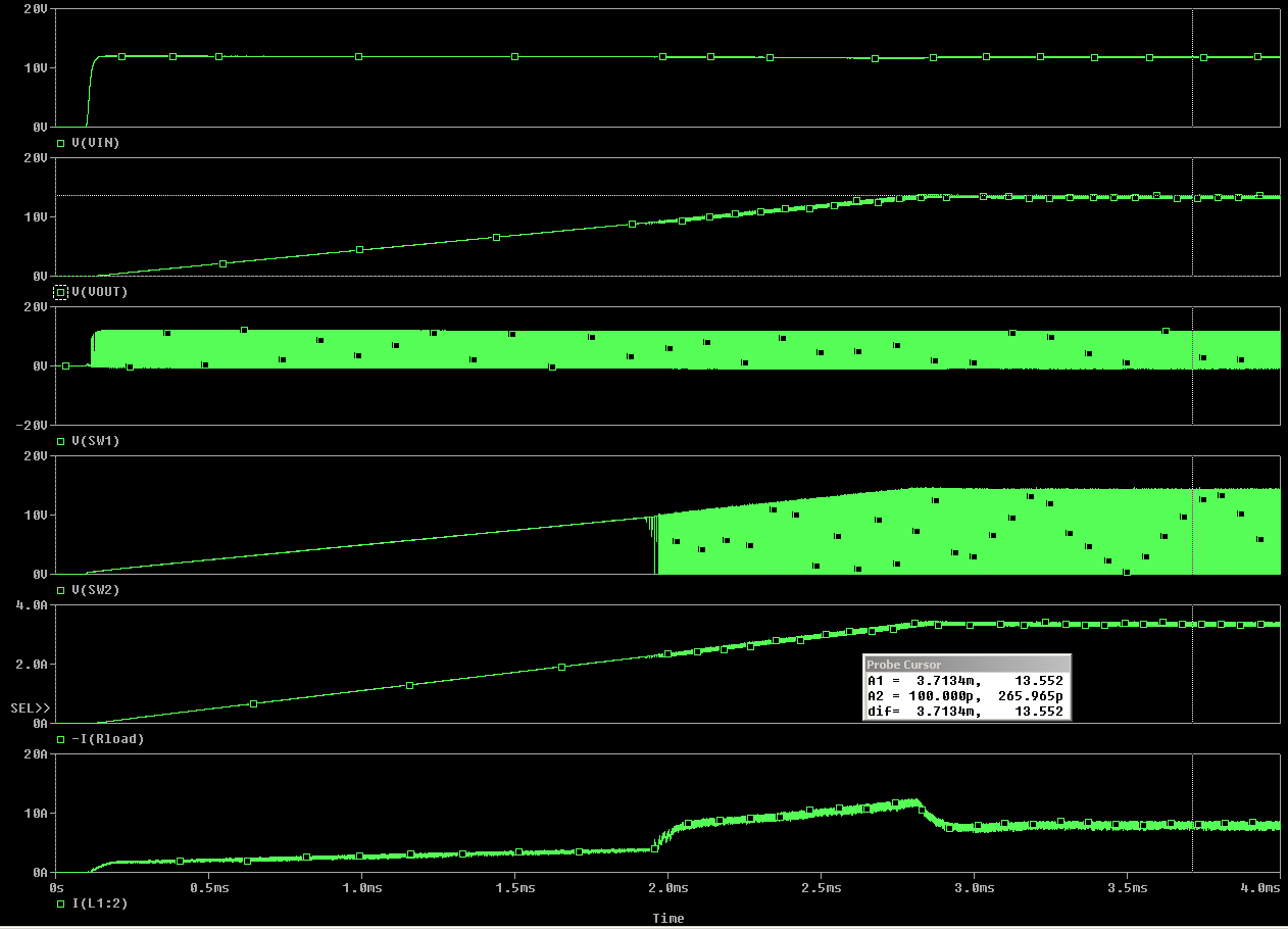
Therefore, I would like to simulate the case1 and case2 with the same design.

And, I would like to know the most suitable design common to both case1 and case2.

Please let me know if you have any advice.

-Case1 Vin=10.8V to 15V , Vout=6.0V , Iout=3.0A

-Case2 Vin=10.8V to 15V , Vout=15V , Iout=3.0A

Regards,

XinYuan Huang

  • Hi XinYuan Huang,

    Please refer the datasheet of LM25118 device. In section 8.2, it is very simple explained in steps as to how one can setup teh external testbench for any VIN, VOUT and IOUT ranges. The example considers 12V VOUT. However, you can use those equations to get values of all components for your requirement.
    Please let us know if there are any further questions.

    Thanks,
    Abhisek
  • Hi Abhishek Tripathy

    The attached file is my schematic for the requirement.

    I am not sure it could work to meet what I want.

    Could help me to check it and provide some suggestions to me?

    3_OK.pdf

  • Hi XinYuan Huang,

    I tried to setup the Pspice released model with this schematic and found that it was able to regulate. Please find Pspice schematic and results below for your reference. 

    Please note that the feedback resistor network used in you schematic sets VOUT at 13.5V and not 15V.

    Kindly revert in case of any further query.

    Thanks & regards,

    Abhisek

  • Hi Abhishek Tripathy

    Thanks.

    I know that.

    My question is how to make Vout is changed from 6.0V to 15V in this SCH ?  Change R16 ?

  • Hi XinYuan Huang,

    In order to change the VOUT, you would require to change the resistor network from VOUT to GND pin via FB pin (R9 and R14 in the above schematic).

    The governing equation is VOUT*R14/(R9+R14)=1.23V (regulation VFB value as per datasheet Electrical characteristics table). So, you can fix one resistor value and calculate the other value based on this equation.

    However, for a single schematic usually the VOUT is fixed and particular values of resistors are used. If you wish to have a single schematic which can support both VOUT values, you would need to make this resistor network capable of changing based on the need.

    I hope this helps.

    Thanks & Regards,

    Abhisek

  • Hi Abhishek Tripathy

    Thanks.

    Does the inductor choke or the others also need to change when I change R9 and R14 in the above schematic ?
  • Hi XinYuan Huang,

    As mentioned above, if you go through the section 8.2 of the datasheet and calculate the schematic components, you would be able to get the recommended values for all of them.

    I did the calculations yesterday for VIN=10.8-15V, VOUT=13.5 (As it was set in the schematic sent by you) and IOUT=3A.
    L came to 16.7uH. Your value of 15uH seems close enough. It should be able to work fine.
    Cout minimum came around 111uF. You have kept 300uF. It should be enough as well.

    However, I highly suggest you follow them and redo those calculations yourself for your exact input and output requirements. That would give you more confidence on your setup.

    Thanks & Regards,
    Abhisek
  • Hi Abhishek Tripathy

    Thanks.