This thread has been locked.

If you have a related question, please click the "Ask a related question" button in the top right corner. The newly created question will be automatically linked to this question.

PMP7760: Problems with aux power series resistor (R112)

Part Number: PMP7760

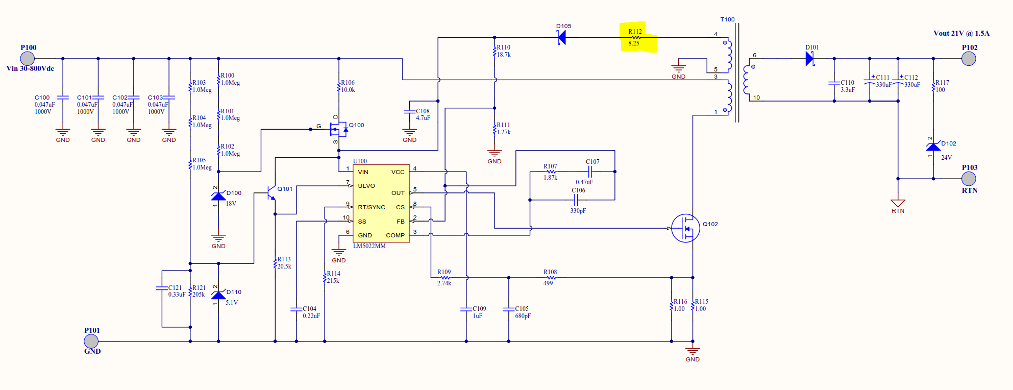
We have implemented an exact copy of your reference design PMP7760, featuring the LM5022 controller, and evaluated it in the lab. The performance is OK when the input voltage is nice and ramps up. But when the power input has excessive impedance (causing instability) or is applied suddenly (high dV/dt), the resistor R112 blows. This in turn causes loss of regulation, which of course is quite destructive on the secondary side. Interestingly, all other components on the primary side survives this.

So my first question is: What is the purpose of R112? How is it calculated, can it be omitted, what power rating should be used?

My second question is: What is the cause of this failure? Whatever happens on the power input shouldn't affect R112 which sits on an auxiliary winding, right? The surge that blows it must either be induced by the transformer or caused by a mysterious strong negative voltage pulse on the Vin node (which I assume doesn't happen since the controller survives the event).

I will perform more measurements but since the failure causes such a mess I want to know what to measure before my next attempt.

Schematic:

  • Hi Filip,

    Thank you for using the LM5022. R112 is usually introduced to damp out any possible resonance between the leakage and C180, because VIN pin is a small load. Its size should be chosen to handle the power dissipation.

    I am still wondering how this circuit would damage withe fast bus voltage application. I noticed that you only posted the schematic from PMP7760 report. May I bother you to post your own schematic when you created your own PCB, just for a quick check?


    Thanks,
    Youhao Xi
  • I appreciate your quick response!

    I have attached the PDF of our schematics. There are a few differences between ours and your, but when the resistor blew the second time, I had removed D6 and shorted L1 and L2, making it more like your design.

    There is also a known error in the schematic: When using the aux winding to power the measurement circuitry, we should tap it from the other side of R1.

    The reason for the 4 power inputs is that we want to measure the voltage without influence from cable resistance. Hence the separate measurement ground "MGND".

    The thing is that when I remove D6, the complexity of this can be disregarded and I think that the schematics is very close to the original design, except that we have extra large input caps.

    Best regards,
    /Filip Wahlberg

    PSU_A.pdf