This thread has been locked.
If you have a related question, please click the "Ask a related question" button in the top right corner. The newly created question will be automatically linked to this question.
Tool/software: TINA-TI or Spice Models
Hello,
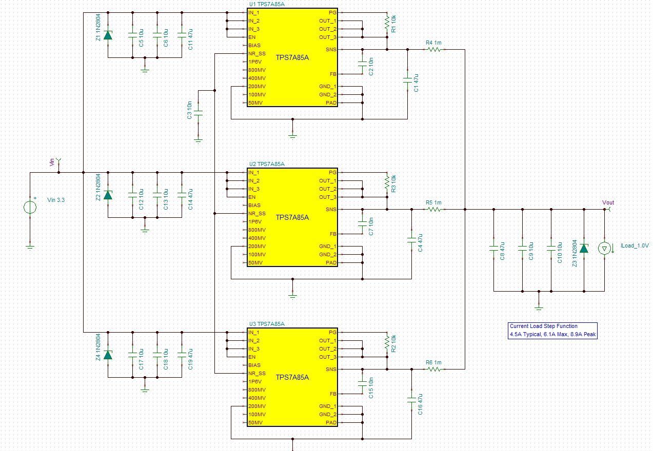
I need a LDO regulator that can provide Vin = 3.3V, Vout = 1.0V and capable of sourcing up to 8A, and upon searching, I found TPS7A85A to be the best candidate. To achieve this high of a current output, it would mean I would need qty 3 TPS7A85A LDOs in parallel. After researching current sharing and LDOs in parallel, TI mentioned that for high current and low noise TIDA-01232 (ballast resistors) should be used, and for high accuracy TIDU142 (control loop and sense resistors) should be used. I am leaning towards using the TIDA-01232 design, due to the fact it has been thoroughly tested with six LDOs in parallel and specifically uses the TPS7A85A; while the TIDU421 design has only been tested with two LDOs and used a different LDO part.
1) If high accuracy is the requirement, is it recommended to use TIDU421 design with qty three TPS7A85A in parallel or is it strictly for only two LDOs? If three is acceptable, how would that be implemented? Would a double supply control loop op amp be needed?
2) I have simulated the TIDA-01232 design in Tina with 3 LDOs in parallel, and wanted to clarify the RBallast and Evout (see calculations below):
In the reference design, there is a given Evout formula, in which I calculated assuming Voutnom = 1V and ERfb = 1% (not sure about this value since it wasn't given or if its needed?)
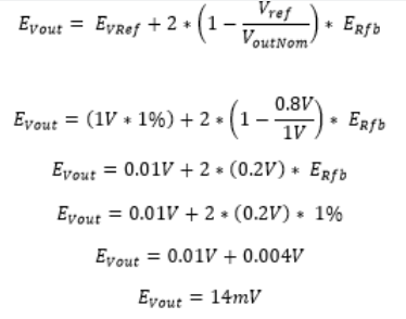
However, in the document it also mentions using Evout = 0.75mV.
I am unsure if I should use the Evout I calculated or the 0.75mV mentioned below.
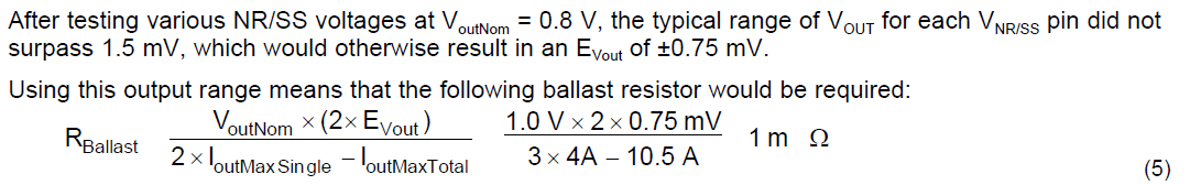
Next, I calculated RBallast using the given formula below. However, I am unsure if this formula is specifically for 2 LDOs in Parallel or if can be used for multiple. If its for multiple then shouldn't the "2" multiplied with IoutMaxSingle be "n", the number of LDOs in parallel? If it is just "2" then I would get a negative result for Rballast.
Note: I Used 0.75mV for Evout for the Rballast calculations because I wasn't sure if I should use the calculated 14mV.
Simulation: Looking at the transient result, it seems like the schematic is designed correctly. I achieved an output voltage of 993.63mV. But would like to know if there are more ways to improve the accuracy of my schematic. Also, is the current going through the ballast resistors supposed to be so small? (probed it with the DMM and current = 5nA for the three ballast resistors)
Hi Dylan,
Yes, you can substitute n = number of parallel LDOs for the number 2 in equations 4 and 5 from TIDA-01232.
Using the attached spreadsheet, I calculated 0.008 ohm ballast resistors.
If you want to correct for the voltage drop across the ballast resistors for better final output accuracy, you can move the output voltage setpoint of each of the paralleled LDOs up. For example, change the output setpoint to 1.02 V. This won't be possible with the ANY-OUT pins, since the minimum step is 50 mV.
There is a blog that describes how to get smaller Vout steps with ANY-OUT here:
e2e.ti.com/.../increasing-resolution-for-any-out-programmable-output-voltage-devices
Thanks Eric, that was very informative.
I have one question regarding the Rballast equation. For the IoutMaxTotal, should that be the total current for the amount of LDOs? For instance, in the ref document it states Ioutmax is 3.5A multiplied by the # of LDOs (see image below), which would be 10.5A for IoutMaxTotal. Calculating for RBallast would then be 20mohms. In simulation I then receive a vout of 968mV, which isn't such a good output.
TPS7A85_TRANS.TSMI also attached the TPS7A85A symbol, you may have to edit the symbol to the way I did.
Hi Dylan,
With the connections described in the ANY-OUT blog, you can change the output to 1.025 V or 1.016 V:
You can achieve 1.025 V output on the TPS7A85A with the following connections:
Connect the 800 mV pin to SNS.
Ground the 50 mV and 400 mV pins.
The 800 mV pin is connected to the internal 2xR resistor. By connecting SNS to 800 mV pin, the 2xR feedback resistor connected to SNS is now in parallel with the 2xR resistor connected to 800 mV pin. This creates a new feedback resistor with value R.
The ANY-OUT resistors are connected in a non-inverting amplifier configuration, so the usual equation applies.
Vout = 0.8 x (1 + (Rf / Rg)), where Rf = R.
For 1.025 V output, the required Rg = 3.56xR.
To obtain 3.56xR, connect 32xR and 4xR in parallel by grounding the 50 mV pin and 400 mV pin. 32xR // 4xR = 3.56xR.
Vout = 0.8 x (1 + (R / 3.56xR)) = 1.025 V.
Since the feedback resistor is now R, each of the ANY-OUT pins will contribute 1/2 of their usual voltage to the output. By connecting 50 mV to GND, you add 25 mV to the output voltage. By connecting 400 mV to GND, you add 200 mV to the output voltage. New output voltage setpoint = 25 mV + 200 mV + 0.8 V = 1.025 V.
_____________________
You can achieve 1.016 V output with the following connections:
Connect 1.6 V pin to SNS.
Ground 50 mV, 200 mV, 400 mV pins.
You can create a feedback resistor equal to (2/3)xR by connecting 1.6 V pin to SNS.
Rf = 0.667xR = (2/3)xR
Vout = 0.8 x (1 + (Rf / Rg)) = 0.8 x (1 + (0.667xR / Rg))
For 1.02 V output, the required Rg = 2.424xR
If you parallel 32xR, 8xR, and 4xR you obtain 2.46xR. This yields Vout = 1.016 V.
I'm attaching the Tina schematic showing both of these examples for 1.025 V and 1.016 V.
Thanks Eric!
So I simulated the output noise of my design via Analysis tab > Noise Analysis
This is the result of my sim:
And this is the datasheet comparison:
My simulated output noise, somewhat looks like the typical output noise from the datasheet. However, I wonder how the datasheet calculated Noise. For instance, figure 18 above, description is 4 LDOs in parallel Noise from 10hz to 100khz is 4.3uVrms. I was wondering how that 4.3uVrms is calculated. I couldn't find a straight forward formula and would like to calculated the overall output noise of my design.
Hello Eric,
Regarding Layout and Placement for the three TPS7A85A in parallel, is it preferred to have the paralleled parts as close to each other as possible? Are their any recommendations for placement of the ballast resistors? Looking at the EVAL board for the TPS7A85A, the two parts look fairly spaced apart.
Hi Dylan,
The TI design used traces on the top layer of the board to implement the ballast resistors, and they are placed next to each other (circled in red):
I recommend a large area fill for Vout, connecting the ballast resistors. With a large fill, there will be minimal voltage drop between the ballast resistors. You can use a tool like HyperLynx to simulate the voltage drops in your board layout from the ballast resistor outputs to the loads on your board.
Hello Eric,
I have another situation regarding improving vout resolution, but this time for vout = 1.8V.
By taking the message you provided above and the blog you referenced, achieving vout = 1.816V is not possible because the range when connecting 1.6V pin to SNS is reduced 0.8V to 1.317V (according to the blog).
So I have considered achieving vout = 1.825V instead, which connects the 800mV pin to SNS providing a two ranges 0.8V to 1.175V and 1.6V to 1.975V. So it should be possible for me to get 1.825 with this method.
calculation: So for Rg I get 0.7805, however, I am unable to get that gain when paralleling the anyout pins. The closest I got was paralleling the 100mV, 400mV, and 1.6V pins resulting in Rg of 0.762.
Not sure if I am calculating something wrong, or if its possible to get vout = 1.825V?
Hello Eric,
In the datasheet under Layout, it mentions several pins such as 13, 3, 8 that are tied to Signal GND. Do you know if the anyout pins require being tied to signal gnd? the datasheet just mentions tying it to gnd. the feedback R2 is tied to signal gnd, so I question if the anyout pins have to be tied also, since they're what sets the output voltage.
Hi Dylan,
Calculate worst case imbalance by margining the outputs. Set one LDO to Vout(nom) + 1% and one to Vout(nom) - 1%. Set the 3rd LDO to Vout(nom).
Vout(nom) = 1.02 V, so margined up output = 1.03 V and margined down output = 1.01 V.
To calculated the Vout (combined), set the 3rd LDO to Vout(nom) = 1.02 V and Iout = 2.667 A (1/3 of total). Vout (combined) = 0.99333 V.
Iout for LDO margined up = (1.03 V - 0.99333 V) / 10 mohm = 3.667 A
Iout for LDO margined down = (1.01 V - 0.99333 V) / 10 mohm = 1.667 A
Worst case imbalance = 3.667 A - 1.667 A = 2.0 A.
Simulation verification:
I wasn't able to get to those output voltages exactly with ANY-OUT, so I went a little higher and lower with margining using ANY-OUT to over-estimate the maximum current imbalance in TINA.
1.041 V: +2% output margining
1 V: -2% output margining
LDO U1 = 1.041 V, Iout = 4.688 A
LDO U2 = 1.02 V, Iout = 2.667 A
LDO U3 = 1 V, Iout = 0.645 A
Worst case imbalance = 4.688 A - 0.645 A = 4.043 A.
TPS7A85A_3_LDOs_Parallel_Ibalance.TSC
For reference, with each LDO set to 1.02 V output, sharing Iout = 8 A equally and 10 mohm ballast resistors, the output voltage is 0.994 V. Each LDO supplies 2.67 A.
Thanks Eric for the detailed response.
Now it looks like I will be needing 4 LDOs in parallel, due to thermal issues not meeting requirement. Therefore, to find the worst case imbalance for 4 LDOs, how would we go about that? would we set the 4th LDO to nominal also?
Hi Eric,
Just for clarification, if i were to use a ballast resistor with 0.5% tolerance instead of 1%. My vout tolerance would be vout +/- 0.5% instead of +/-1% correct?
so voutnom = 1.02V, vout margined up = 1.025V, and vout margined down = 1.015V.
Eric,
Thank you.
Since the 4 LDOs in parallel is almost complete. I do have questions regarding 2 LDOs in parallel. It seems like the control loop method (TIDU421) because it provides high accuracy at the output and better current sharing. Looking at the TIDU421 design, it is using a different LDO and the components chosen seem to be specific to that LDO. Since i am looking to use the TPS7A85A instead, how can I be sure the I am choosing the right op amp (document states "Care must be taken to choose op amp with appropriate CMRR voltage range"), as for the feedback resistor they chose 15k, but doesn't show any calculations for choosing that value. And as for the sense resistor, they said a nominal value of 30mohms or less should be used, are there any calculations that support this? Will this value be okay to use for my application?
I tried implementing the tps7a85a part with the control loop and sense resistor in TINA TI, and the transient waveform is not what I expected. Huge ripples. I believe it may be something to do with the op amp, when not tying the negative to ground and power supply to VIN, the transient waveform is what I expect although the positive and negative supply must be used to power up the op amp.
Eric,
Okay, thank you.
I tried implementing the tps7a85a part with the control loop and sense resistor in TINA TI, and the transient waveform is not what I expected. Huge ripples. I believe it may be something to do with the op amp, when not tying the negative to ground and power supply to VIN, the transient waveform is what I expect although the positive and negative supply must be used to power up the op amp.2538.TPS7A85A_Parallel_VOUT_1V_LIN_Control Loop.TSC
Hi Eric,
This is what I have for placement regarding 4 LDOs in parallel, and this is the amount of room that I have on the board. Are their any concerns with the way I laid out the components? I don't have much room to space out the LDOs the way the eval board does. Also this is how large of an area fill that I have for the output voltage connecting the ballast resistors. Is this enough?
Thanks for response Ryan regarding the 15k resistors.
Now how are the sense resistors calculated? along with the resistors at the input of the op amp?
I know for the TIDA-01232, the document gives us the formula for calculating the ballast resistors. I was hoping maybe we can get into that kind of detail regarding the sense resistors.