This thread has been locked.

If you have a related question, please click the "Ask a related question" button in the top right corner. The newly created question will be automatically linked to this question.

PMP22557: PMP22557: Change the design to 5V output

Part Number: PMP22557
Other Parts Discussed in Thread: UCC28730

Sorry I come back the old topic "PMP22557: Change the design to 5V output" which has been locked after a so long time.

This topic is supported by John Betten.

Hi John,

I am back again and sorry for not giving response for you last reply due to this project is on hold for other urgent project, and now we are resuming it

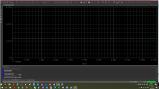
I make the simulation today with pspice for TI and the result shows the out is almost 0v, only about 20uV, I attached the project file here can you help to simulation and check it?

Thanks

UCC28730.zip

  • Hi Rick

    I think the root cause is the CS RES wrong value, it should be a RES < 3.2ohms, while you choose a 2.4k for R17 is too large.

    It will be a OC fault during the start up.

    And here are some advice for your simulation:

    follow below steps to check your simulation circuit :

    • Make sure that your connection is totally right and all the diodes direction is right;
    • Check your CS RES value is correct;
    • Check your feedback divider RES value are correct;
    • You can confirm your Res and Cap design and return to John recommendation before.


    Best regards,

    Mia Ma

  • Hi Rick,

    Just we have noticed that PMP22557 design is not proper for a 5V output,  the circuit could not work.

    In PMP22557 design, VDD supply is charged by Vout through D1 and D2 while Q1 is ON. As you want 5V output, and considering of two diode forward drop, the VDD voltage is lower than Vvdd(off) minimunm value 7.3V. So the circuit couldn’t work and will enter a UVLO fault.

    So please change the design back to a Flyback topology, and you can refer to the UCC28730 EVM design:  https://www.ti.com/lit/pdf/sluub75

    Best regards,

    Mia Ma

  • Hi Mia Ma, Thanks for the reply

    Yeah, got it, VDD is suggested about 9V in the datasheet. So I would reuse the standard 12V design. But the output is still abnormal

    Attach the 12V simulation project file here

    2388.UCC28730.zip

  • One more question about PMP22557 design, while the NPMOS is on, the sw node will equal VIN, how the drive bootup a very high voltage than VIN since VIN is more than 150V?

  • Hi Rick, 

    1. therw will be a library error in my side, so please confirm you simulation setting by youself. There is no value error and you can refer to following resource:

    https://training.ti.com/pspice-ti-brief-overview?context=1146489-1146487-1147384 

    https://www.ti.com/lit/pdf/tidm694 

    2. The drive bootup understanding:

    The VDD cap is charged during Q1 is off, and D3 is on, UCC28730 GND pin is right connectted to output GND through D3,  so the 12Vo will charge through D2 and D1. And while Q1 is ON, D3 is off, voltage on C1 will drop a little because of no charge. And during next D3 on stage,Vdd will be recovered.

    What you are confusing here the point  is that the DRV or VDD voltage is compared to the UCC28730 gnd pin, which is exactlly the SW node. So whatever the SW node voltage is, it's no matter with the voltage delta (ΔV) of C1(Vdd) and DRV to GND PIN(Vgs).

    Thanks

    Best regards

    Mia Ma

  • Understood ,thanks, the simulation file is ok for me, but the NMOS and Inductor models are not from tool library , I put them in the zip file attached, you want to add them to the design by editing the simulation profile->configure files->library files and then select the file and add to design.

    As this is a special design, I would like to see simulation result before release our board.

    1768.UCC28730.zip

  • Hi Rick,

    As your design is roughly totally same as PMP22557, there is no error. So you could complete your design referring to PMP22557 directly.

    We are focusing on device design and application, not simulation detail. So if you have more confusing item of this part or its application, it will available for us to answer it.

    Thanks.

    Best regards

    Mia Ma