This thread has been locked.

If you have a related question, please click the "Ask a related question" button in the top right corner. The newly created question will be automatically linked to this question.

CC2652P: CC2652P1FRGZR

Part Number: CC2652P
Other Parts Discussed in Thread: CC1352P, TPD1E04U04

Tool/software:

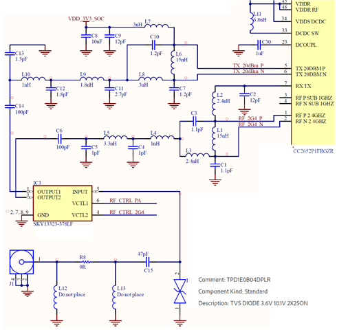
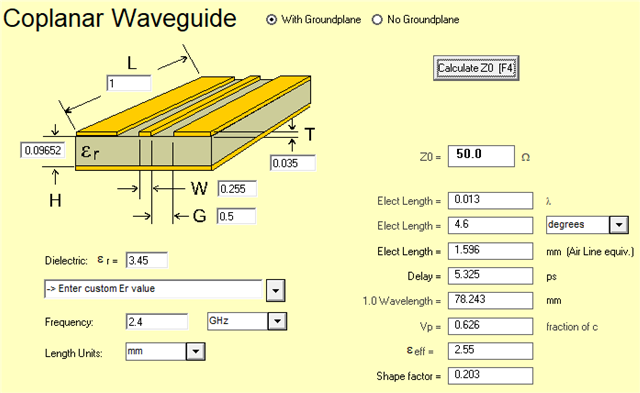
I’m currently reviewing a legacy design for BLE 5.2, 2.4GHz (schematic attached) that may be experiencing issues related to impedance mismatch, sensitivity, or low output power on both RF ports (low power and 20 dBm). The antenna in use is a Taoglass PC.11.

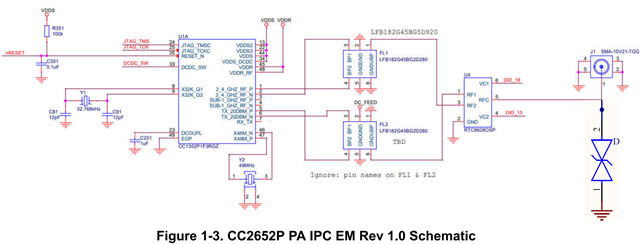
Can anyone confirm whether the selected matching component values are optimal? Should an Integrated Passive Component (IPC) be used on both RF ports? If so, what IPC is recommended for the CC2652P, particularly for the 20 dBm high-power port?

I can also share the PCB layout if needed. An S11 analysis using a VNA and output power measurements with a spectrum analyzer are planned.

Thanks for answering.

  • Hi,

    Please can the customer share more details of their measurements and what the exact issue(s) they are observing are?

    When they say that the design

    may be experiencing issues related to impedance mismatch, sensitivity, or low output power on both RF ports (low power and 20 dBm).

    we would need more information to be able to start to identify a root cause.

    Regards,

    Zack

  • An additional point, please submit any design review requests using: 2.4 GHz Design Review Submission: https://www.ti.com/tool/SIMPLELINK-2-4GHZ-DESIGN-REVIEWS 

    A quick issue to flag is that the DC blocking capacitors C14 and C6 should be 47 pF for 2.4 GHz. However, without more information on the issues you are seeing it is difficult to know if correcting those would make a large difference or not.

    Regards,

    Zack

  • Hi Zack,

    Apologies for the delayed response, and thank you very much for your feedback — it's truly appreciated. We're currently waiting to receive the board, after which we'll begin debugging and run the tests I mentioned. Once we have the results, I’ll be sure to share them here.

    Thanks again!

    Regards.

    Carlos

  • Hi again

    I was in the lab today measuring the RF output power using the BOM as shown in the previous schematic. When setting the output power to 20 dBm in the firmware, the measured output was around 17 dBm, indicating approximately 3 dB of losses.

    I also checked the S11, which was initially around –4 to –5 dB. I then adjusted C11 and C12 to improve the impedance matching, and managed to bring the S11 down to –10 to –15 dB. However, I noticed that the output power dropped further to 15 dBm after this adjustment.

    Do you have any idea why improving the S11 would lead to a decrease in output power? I would have expected the opposite behavior.

    Best regards,
    Carlos.

  • Hi Carlos,

    Relying only on S11 measurements is not the recommended route for power matching. The identified optimum load impedance is a compromise between many factors (detailed in Section 9 of SWRA640 (CC13xx/CC26xx Hardware Configuration and PCB Design Considerations): https://www.ti.com/lit/swra640 ).

    It is likely that your design is deviating from the TI reference design and it is is best to minimise the differences before focusing on tuning the matching network further; did you submit your design for a review using the portal linked above? I can follow up on that if so.

    Additionally, please detail how you performed the measurements (e.g. did you use SmartRF Studio 7 to program the device to transmit a CW wave).

    Regards,

    Zack

  • Hi Zack,

    Thanks for your detailed reply.

    We will definitely take your recommendations into account, as we are currently deep into a critical and time-sensitive phase of the design.

    Regarding the design review: we intend to submit the design through the TI portal, but our management requires an NDA to be signed before sharing the full documentation (BOM and Gerbers). If progressing with the NDA is not possible in a timely manner, I would kindly ask you to consider the schematic I shared previously for now.

    As for the measurement setup: I used SmartRF Studio 7 to configure the device to transmit an unmodulated Continuous Wave (CW) across all channels. The signal was then measured directly using a spectrum analyzer.

    Please let me know if you need any additional details on the measurement setup or the hardware configuration. Our main goal is to maximize the output power with minimal PCB modifications, ideally just by adjusting the values of discrete components in the matching network in both ports (20dBm and low power).

    Thanks again for your support.

    Best regards,
    Carlos Arroyo

  • Hi Carlos,

    As for the measurement setup: I used SmartRF Studio 7 to configure the device to transmit an unmodulated Continuous Wave (CW) across all channels. The signal was then measured directly using a spectrum analyzer.

    At what point in the RF path are you measuring?

    I would strongly suggest comparing your BOM to the reference design yourself and removing/minimising any differences, including using the recommended component vendor series if possible - for example, C14 and C6 should be 47 pF as previously mentioned. The PCB stackup should also match the TI reference design, especially the dielectric thickness between Layer 1 and Layer 2 (this is very important).

    Regards,

    Zack

  • Hi Zack,

    Thanks for the details.

    The output power was measured at the antenna connector J1 (please refer to the schematic at the top of the thread).

    Regarding the reference design — could you kindly share the exact link? I’ve tried to locate it but haven’t been successful so far.

    As for the PCB stack-up, in our case it’s fixed (please see the image below), and unfortunately we cannot modify it. Could you advise on what implications this might have, particularly in terms of matching performance? And based on that, which component values or trace widths we should adjust accordingly?

    Best regards,
    Carlos

  • Hi Zack,

    Following up on my message from yesterday, I wanted to ask your opinion regarding a few modifications we're considering for our RF design. While we’re generally following TI’s recommendations (from Application Note 2.4-GHz, 10-dBm PA IPC for CC26x2P and CC1352P, https://www.ti.com/lit/an/swra729/swra729.pdf?ts=1750230858305&ref_url=https%253A%252F%252Fwww.google.com%252F ), we are evaluating the following changes:

    1. Using IPC components (specifically the LFB182G45BG2D280) instead of discrete L/C matching components.
    2. Replacing the RF switch with the SKY13323-378LF instead of the RTC6608OSP.
    3. Adding an ESD protection diode (TPD1E04U04, 0.5 pF) from the antenna trace to ground.

    From your experience, do you think these changes could significantly affect TX efficiency, RX sensitivity, (As you said before S11/matching doesn't matter)?

    Thanks in advance for your feedback.

    Best regards,

  • Hi,

    The design files are found here: LAUNCHXL-CC1352P-2 (SWRC350): https://www.ti.com/lit/zip/swrc350

    The +20 dBm HPA path and the standard 2.4 GHz, +5 dBm path are the two to use for your application.

    Your PCB stackup deviates from the 0.175mm dielectric thickness between Layers 1 and 2:

    This will change the required impedance matching for optimal performance. Without simulating your PCB and/or performing load-pull measurements it is difficult to say how you should modify the matching network.

    Regarding your other questions:

    1. Using IPC components (specifically the LFB182G45BG2D280) instead of discrete L/C matching components.

    You can use the IPCs, but you will need to add the footprints for an additional PI network after each IPC (before the RF switch) so that you can account for the change in PCB stackup. Otherwise you will be stuck with the performance that the IPCs provide with no way to change that.

    So, it depends on whether you can change the design to follow the TI reference design as closely as possible (mainly the stackup, which it sounds like may not be an option for your application).

    It would still be a more compact design, but more difficult to adjust as there are fewer degrees of freedom.

    2. Replacing the RF switch with the SKY13323-378LF instead of the RTC6608OSP.

    This is fine, the performance might actually be improved (but the Skyworks RFSW has a higher associated cost).

    3. Adding an ESD protection diode (TPD1E04U04, 0.5 pF) from the antenna trace to ground.

    We have tested the TPD1E0B04DPY on the LAUNCHXL-CC1352P-2 reference design, so would recommend that ESD protection diode. It may add a few dB of spurious emissions, but the performance was acceptable during characterisation.

    Regards,

    Zack

  • Hi Zack,

    Unfortunately, we are unable to modify the PCB stack-up. As a result, we’ve adjusted the trace width in your design to 0.255 mm (see image below). For this version, we will maintain the RF tracks and schematic as they are—using discrete components rather than the IPC balun—and only replacing the 100 pF capacitors with 47 pF ones.

    Due to equipment limitations, we’re currently not able to perform load-pull measurements. However, we are conducting S11 and output power measurements. Would you be able to suggest a target S11 value we should aim for in our design?

    Best regards,
    Carlos

  • Hi Carlos,

    Unless it is a large order I will not be assigned the time to simulate this - do you have the tooling to simulate PCBs yourself?

    Regards,

    Zack

  • HI Zack,

    The only tool available to me is AppCad, if that can be considered a simulation tool. If you're referring specifically to tools like ADS, HSS, or Microwave Office, unfortunately, we do not have access to those.

    Regards.

    Zack

  • Hi Carlos,

    You mention that you are considering changes to the RF design, but I am a bit confused.

    Are you trying to modify the existing design with a BOM change only to regain the RF performance, or can you make additional changes? If the latter, what elements are you able to modify?

    Regards,

    Zack

  • Hi Zack,

    Thanks for your message.

    Our goal is to achieve the best possible output power and reception performance, and to that end, we are carefully following your recommendations.

    For this first iteration, we will limit the changes to replacing the 100 pF capacitors (C6 and C14) with 47 pF as you suggested.

    For future versions, since we are constrained in terms of simulation tools and cannot rely on TI support due to internal restrictions, we plan to explore using the Murata balun on both RF ports. We would also consider adding a PI matching network afterward, as you previously recommended, to further optimize the performance. 

    We’d really appreciate your opinion on this approach — do you think it’s a reasonable direction to take given our constraints?

    Best regards,
    Carlos

  • Hi Carlos,

    I think you'll have similar issues with either approach; the change in dielectric thickness between Layer 1 and Layer 2 will require a rematching effort. The IPC still contains the balun and LC matching, so you could get additional filtering of spurious emissions by adding the Pi filter, but either way you will effectively be attempting the same thing.

    If you can't change the PCB stackup but can add extra components to the LC filter, I would follow the (preliminary) design for the LP-EM-CC2674P10/cfs-file/__key/communityserver-discussions-components-files/538/LP_2D00_EM_2D00_CC2674P10_5F00_Preliminary.zip

    This will give you the most flexibility in the design, but you will probably still need to account for the change in board thickness through tuning.

    If you have a VNA available, you can directly measure:

    • The balun performance on your board and the balun performance on a TI reference design. You can then double-check that the balun on your board performs acceptably (good CMRR in the passband, similar impedance transformations, etc.) and directly compare the S11 match at the balanced and unbalanced ports.
    • The LC filter on your board and a TI reference design for comparison.

    If you treat the balun section as "fixed", you can try to adjust for the measured performance deviations between your board and the TI reference design.

    If you have limited tooling, adjusting the shunt capacitors in the LC ladder network could help you regain performance.

    Measuring performance at the SMA output as you vary the capacitor values should allow you to build up a rough picture of the target impedance - the performance will be optimum 

    This is not data for the CC2652P, but the general behaviour of the load-pull plots shown below will still be seen. Even if the locations of the Output Power and current consumption contours change, the concentric behaviour of the Output Power contours and the trend of low-to-high current consumption regions will remain similar:

    So, you can roughly "map" the contours - if you reach a region of unacceptable performance in one impedance trajectory (e.g. by increasing/decreasing a particular component value), note the impedance trajectory measured on the Smith chart using the basic simulated networks. That would build a (very) rough picture of the performance - e.g. the output power could increase as a specific capacitor value is increased, then decreases again (with accompanying variation in current consumption/efficiency). It's not perfect, but you can then at least try and avoid targeting the same load impedance repeatedly with different BOM values.

    Regards,
    Zack

  • Hi Zack,

    Thank you for your message and clear explanation.

    To summarize your recommendation: since we cannot modify the L1/L2 dielectric thickness, your proposal is to follow the design from the LP-EM-CC2674P10 reference. Then, once implemented, we should measure the balun performance and proceed with tuning the LC network—starting with adjustments to the shunt capacitors—to compensate for any impedance mismatches and regain performance.

    We’ll move forward with this approach and I’ll keep you informed as soon as we have the new PCB version ready and measurements available.

    Thanks again for your support.

    Best regards,
    Carlos