This thread has been locked.

If you have a related question, please click the "Ask a related question" button in the top right corner. The newly created question will be automatically linked to this question.

CC2640 Custom Board Design

Other Parts Discussed in Thread: DRV2603, CC2640

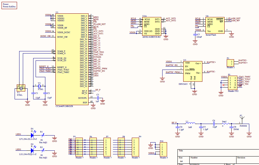
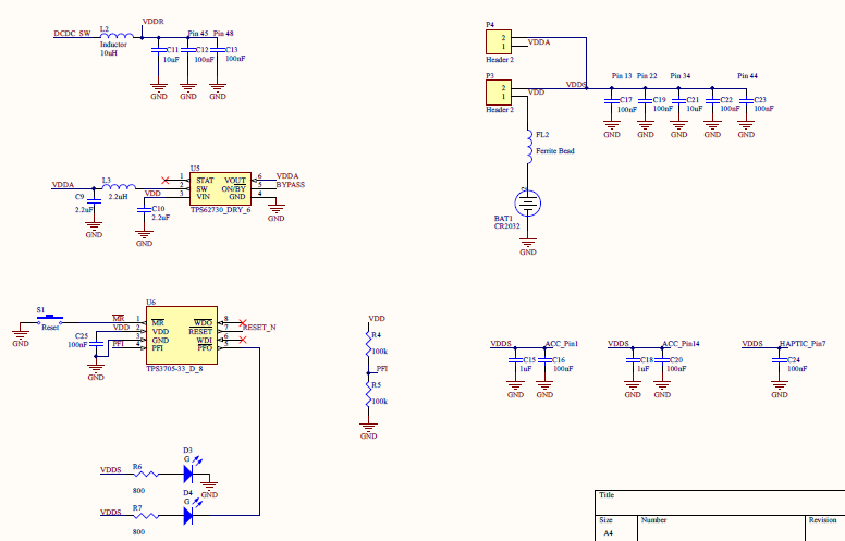
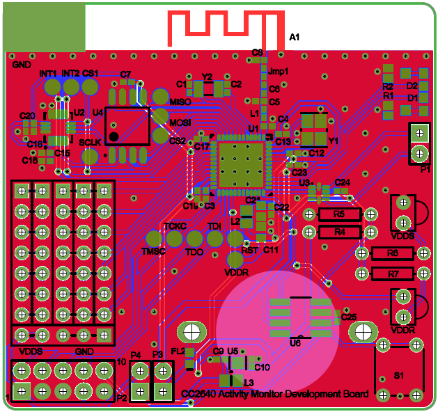
I have designed a custom board for a final undergraduate project using the CC2640, accelerometer, serial flash and DRV2603. I have a pcb mill with no through hole plating so the QFN package has been a challenge. I had some issues with my first revision so I have done a second revision. I would really appreciate someone having a look to see that all is in order. I am using the CC-DEVPACK-DEBUG so have broken out to a 5x2 header. Power is supplied via crocodile clips on the LHS of the board or header P8. Please find the schematic and layout in this pdf.

Thanks

  • What kind of issues did you have with your last design? Your new design looks ok, even though the grounding is not optimal. This might reduce performance. I would have liked to see more vias, especially for the RF components, the decoupling caps and the large DCDC capacitor. Pin 34 needs a 100 nF close to the pin in addition to the 10 uF capacitor. Optimal routing for the decoupling capacitors is VDDS to capacitor pad to the pin it is to decouple, but your lines to the decoupling caps are so short so they are ok. Note that you can make have external bias for your design using the other RF pin for biasing if you want to gain 1 dB sensitivity. For the RF components, I would rotate C4 180 degrees to reduce the leakage between C3 and C4. Also note that you can order small amount of PCB quite cheap from different producers in China, for instant Seeed Studio and Itead. This might be less work for you and your design can be further optimized. 

  • Charlotte,

    Short summary for the issue Cameron had with previous design is that device did not get power up properly. Measured VDDS level was 3.3V but nothing comes out from VDDR.

    You can find the discussion and design files here
    e2e.ti.com/.../443765
  • Thanks . I do not know what they layout differences are, but making your own PCB and hand mounting the chip is not straight forward. As I said, even with your new design, grounding is far from optimal.
  • Thanks for your responses.

    I'm not sure how I missed that 100nF cap on pin 34, will add it.

    As Christin Lee pointed out, my main problem was incorrect voltage levels which suggests poor soldering of the CC2640. I had a new chip put on and somehow ended up with a short between DCDC SW and VDDS and no step down conversion to VDDR either. I have altered the footprint of the CC2640 to so it has one 2mm hole to solder directly to the EGP. (1) Is this a bad idea?

    The other problem was copper delamination at the vias and headers since they were just too small. In this design I have increased the diameter of the copper which has made them very big and hard to fit in. This is why there are so few of them. I placed one at each set of decoupling capacitors, I will move the via closer to the DCDC components. (2) How else would you suggest improving grounding?

    I am not really sure what an extra 1dB translates to in terms of performance. I do not need long range at all, 1m would suffice. (3) Would the external bias be worth it?
  • The holder under the chip is a good idea, and I see that you have done your best you can with the tools you have. My point was just that making a design in this way is always a risk, but you have a good chance that it can work. No need to add the external bias if you do not want it, it gives 1 dB better link budget (better sensitivity) but for the range you require, you should be fine without it:)
  • Great, thanks very much for the feedback. The lack of solder mask is more than likely the main cause of my issues. I will leave the soldering to a professional and hope for the best. Worst case scenario I will have it manufactured, I am just trying to avoid having a design made that I am unsure of.
  • I hope I can revive this thread, I haven't had success. I had the board carefully soldered up under microscope and tested every trace for shorts between each other and to ground. All seemed in order so I applied 3V from a power source but didn't set the current limit so it was around 300mA. After less than 2 seconds the power supply indicated there was a short. Now pins 44 (VDDS) 45 (VDDR) and 48 (VDDR_RF) are grounded. So I presume the chip is dead.

    I don't understand where I've gone wrong, I simplified the design as much as possible and only soldered in what was needed to connect with the debugger. This is the schematic for the connections I made:

    Any ideas? I am willing to have a proper board manufactured but not if I am going to end up with the same problem...

  • It is hard to say, the schematic is ok and the layout looks ok, however making a board in this fashion is not easy. can you send a picture of your board? Getting the correct amount of solder paste underneath the chip is tricky, you need enough to get good grounding but not to much so that the chip looses connection on some pins. Making a design this way is as said earlier high risk, and I would recommend getting the boards produced. We can review schematic and layout in advance.
  • I have had a new board made professionally. I have used the TPS3705-30D to monitor voltage levels and control the reset. I wanted to solder on as little as possible and check the voltage levels since that is the problem I had before. I soldered the decoupling caps, buck converter components and crystals. I got +-0.6V at VDDR and +-0.3V at DECOUPLE (Pin 23). I am using all new components and had the CC2640 chip put on by a professional. Admittedly I realised afterwards that leaving off the TPS3705-30D meant that the RESET pin was left floating, would this affect the buck converter? My TPS3705-30D chips arrive tomorrow, please have a look at my design, I followed reference design very closely for power layout.

  • So the floating reset was the issue here. Go here for more endless problems.