This thread has been locked.

If you have a related question, please click the "Ask a related question" button in the top right corner. The newly created question will be automatically linked to this question.

CC2640 PCB Design comprobation

Other Parts Discussed in Thread: CC2640, TPS782

I'm doing a redesign of my cc2640 board following the suggestion of TI engineers and i need some help to know if i'm doing it well or is something wrong. The list of things i have to improve in my old desing was:

- Add antenna tuning components:

I added an extra inductor and now RF frontent is with external bias. 


- All RF comp should have separate vias to GND.

I don't understant what that means. It means that the RF have to have separate ground planes?, or only vias? because the old design have separate vias or i'm missing something. Also in the Ti referecne desing i don't see separate gorund planes for RF components.


- There should be no routing between decoupling GND vias and the vias under the chip.

Now there is direct path from decoupling capacitor vias to the cc2640 ground vias.

- Routing under the crystal traces is not recommended

I change the path of VDDR and now there isn't any trace behind crystal signals.

- Distance from the RF pins to comp should be kept to a minimum.

I put the RF components the closest as posible to the cc2640


- Decoupling caps should be placed close to the pin it is to decouple.

I think in the old design have the decoupling capacitor close, but i tried to put them as close as posible too.
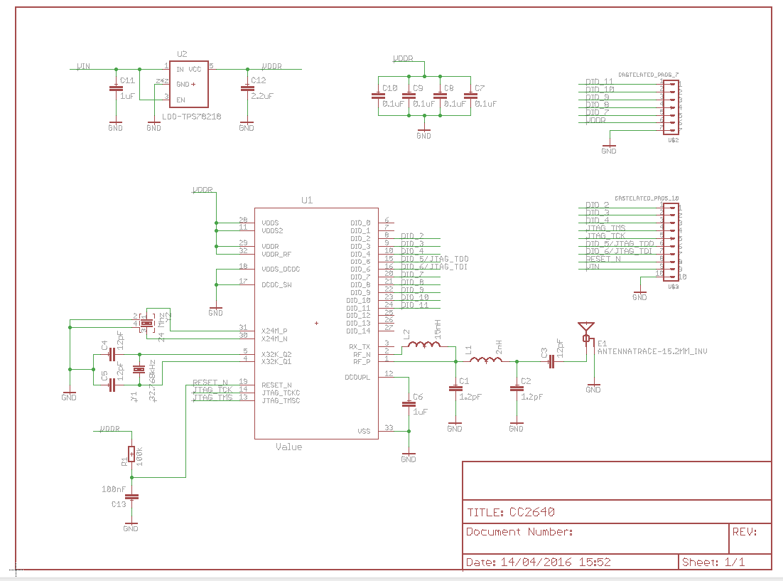
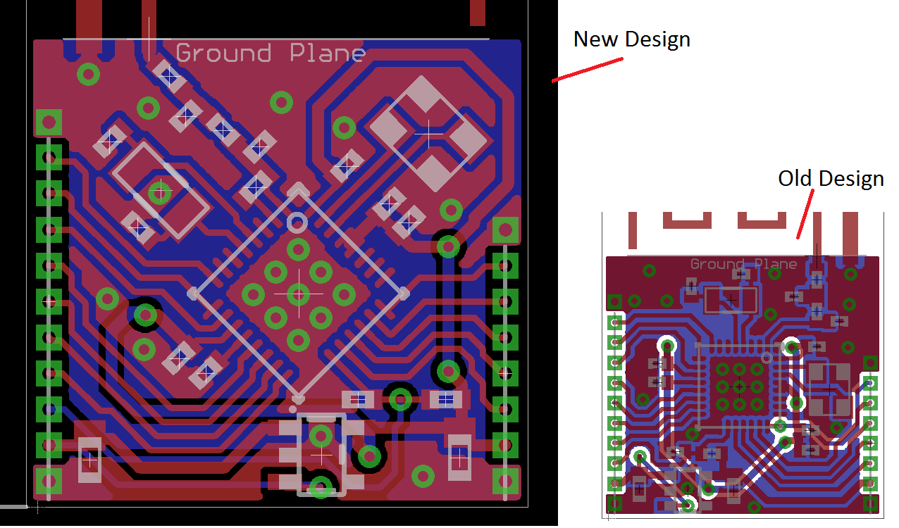
Can you check is the design is correct or if i need to change something before i send it to fab?

I undesrtant that with a image is dificutl to check the design. If you need more info i can make more images or send you the files.

Thanks. 

  • I see that I was a bit quick in my initial comments on your design. This was because, as said in your previous post, I do not believe they are related to the issue you were experiencing with noise on the power. Have you gotten any feedback on the external LDO you are using from the other team? Your intitial layout is not that bad, my comments where most in case you got performance issues (no need to fix what is working).

    I see that you have changed your front end configuration to single-ended with external bias, this will give you 1 dB better sensitivity. That was however not what I meant with placeholders for antenna tuning components. The impedance of the antenna will depend on the size of the pcb, casings etc and must be tuned to be 50 ohm. we normally recommend adding placeholders for a series and a shunt comp close to the antenna to be used for this purpose. You will see that in our reference designs using the same PCB antenna you use, have different tuning or length in different TI reference designs. For more info, see also AN058 www.ti.com/.../swra161b.pdf

    Your decoupling and grounding is better, but I see I was not clear on my point on GND vias. No need for separate GND planes. Have you looked at this: processors.wiki.ti.com/.../CC26xx_HW_training_Layout_Considerations.pdf and this processors.wiki.ti.com/.../CC26xx_HW_Checklist In point 3 in layout you see this:
    3: All RF components connected to ground should have multiple ground vias close to their ground pads to minimize ground impedance.
    In your design there are several components "sharing" a GND via for instant pin 11 and 12 decoupling caps and the decoupling for pin 28 and 29, there are no GND vias for the ground pads of the crystal and crystal loads, and the shunt comp in the RF trace towards the antenna should have more GND vias close to their GND pads.
  • Hello CHS,

    Frist of all, thanks for your help, i really apreciate it. The other team answer my about the LDO, the problem is the transient response of the TPS782, because is a very low quiescent current, his respode is "slow". But they said that with extra capactity the problem should solve, and that is strange the need of such high capacity (100uF) in my tests. They suggest my other LDO so i'll do more tests to find the problem.

    About the PCB design, i have time while i'm waiting for the new LDO to test, so i'll do the sugestions you said and i'll post the PCB again for you to give me the green light.

    Thanks.

  • Hello,

    I have an extra question. I need to improve the range of the module. The new design have external bias and the documentation says that it improves the sensitivity from -94 dB to -96 dB with only an extra inductor. My question is, si worth trying the diferential output with external bias for only improve the sensitivity from -96 dB to -97dB?, what improvement in range i can see if i do it?

    if i keep the design single ended with external bias, witch is the improvement in range form the previous one (single ended with internal bias).

    I know that the range depends in other factors like antenna design, PCB, ... but i need some aproximation, like inprovement in percetage of the range or something.

    Thanks.
  • I suggest that you test our range tool, e2e.ti.com/.../375823 to help you decide on what front end configuration to use. theoretically, 6 dB better link budget should double the range.
  • I'm using the excel from the link you give me, i choose the cc26xx but i can't change the sensibility to match the sensibility of the diferent antenna components. Is there any way to change this, so i can't measure the diference in range with some components and with others?

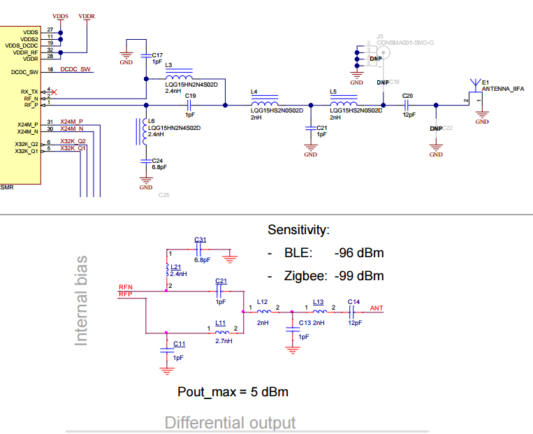
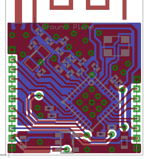
    And other question. I saw that there is a diference in rf pins in the referecne designs. For example in the temperature sensor example the RF_P and the RF_N are swaped from the RF Frontend options pdf:

    i gues the order doesen't matter but i have to be sure.

    Thanks.

  • Change the output power instead of the sensitivity, it will have the same affect in the range tool.

    And you are correct, the order of RF_N and RF_P when using a balun does not matter, what is important is too keep the layout symmetrical when using a differential configuration.
  • Hello,

    I made some changes to the previous design and i made a new one with diferential output, i will send to fab the two modules for prototyping and to test which one i will use at the end:

    you said is important to keep the layout symmetrical, you mean components and traces, it's ok in the design i made?

    Thanks.

  • If you mirror the balun in the differential board you can use external biasing which will improve sensitivity by 1 dB. With the setup you have now, you will get the same sensitivity on both boards.

  • but with the single ended design i can only configure the output power to a max 2 dB, and in the deferential mode i can configure it to a max of 5 dB, or i'm wrong?
  • That is correct.

    I was only pointing out that with the current differential layout you will get the same sensitivity between the two boards, and that you can easily improve the sensitivity on the differential design by 1 dB.
  • My final design ->  Diferential with external bias:

    I have one final question, the turn in the trace between the blaun and the PCB antenna (between the last component an the antenna) can affect the performance?

    Thanks.

  • Looks good. The last turn before the antenna is ok. There are still no antenna tuning components though, but I see that there is not much room for it either.