This thread has been locked.

If you have a related question, please click the "Ask a related question" button in the top right corner. The newly created question will be automatically linked to this question.

CC2564: Pinout of CC2564 in YFV package ( R-XBGA-N54)?

Part Number: CC2564

I need the pinout of the CC2564 in the YFV  BGA 54 package.

The BGA mechanical drawing is shown in the datasheet on page 51, but no pinout table is given.

The datasheet only has the RVM  VQFN-N76 package pin functions.

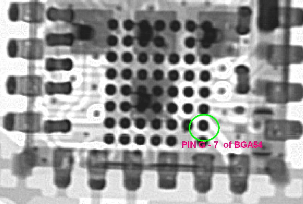
We have X-rayed a BT module from LSR which uses the BGA-54 package.

We need to know the pin mapping to troubleshoot an issue with this BT module.

Specifically we need the function of pin G-7 on the BGA. 

I can send picture if that helps.

Regards,

Mike Kirk

Kenall Mfg.

  • Here is the X-ray showing the pin of interest:

  • Hey Michael,

    I'll look into this and get back to you soon.

    Thanks,
    Seong
  • Hey Michael,

    Pin G-7 of this package is GND.

    This package is NRND which is why you are unable to find any information online.
    The mechanical drawing and part numbers that is currently in the datasheet will be removed soon.

    BR,
    Seong
  • Hi Seong,

    Thanks for looking into this. From our X-ray, the pin G-7 appears to be wired to pin 6 of the CC2564MOD Bluetooth module.
    Can you confirm this to be true?

    If yes, I am confused, because pin 6 is listed as No Connect for this module, not ground.
    I confirmed in a previous TI support ticket that this pin cannot be grounded, it must be No Connect. So I am trying to clear up the confusion. Pin 6 is no connect or ground?

    We wish to use the CC2564MOD part as a 2nd source to the LSR TiWi-uB2 Bluetooth module which has same pinout (except for pin 6) and same package footprint. LSR uses older TI 2564 chip (not 2564B) - so we know the patch firmware is different.

    BR,
    Mike
  • Here is reply from Vihang from April 2018:
    =========================================
    Apr 20, 2018 3:46 PM
    In reply to Michael Kirk:

    Hi Michael,
    The Pin 6 on the CC2564MODN cannot be grounded. It should be left NC.

    Michael Kirk
    I should add that both modules use same TI CC2564 dual mode BT chip.

    CC2564MODN has the CC2564B IC inside it. To best of my knowledge, the LSR module has the first generation CC2564 device inside it. Both CC2564 and the CC2564B require different firmware service-packs. So even if these two modules were exactly pin-to-pin compatible, the one cannot act as a second source for the other without changing your host side firmware to incorporate the respective service-packs.

    Best regards,
    Vihang
  • Any update on this?

  • Hi Michael,

    I hope all is well. My apologies for the late reply as I looked into this. Inside the CC2564MODN is the CC2564B IC. Pin G7 is in fact pulled out to pin 6 on the Module package. This was a pin with and old feature that is not being used.

    When you place the module on your PCB, pin 6 should be left as a NC. It should NOT be GND. this is also in accordance to what Vihang had previously stated as well as our reference designs for the CC2564MODN.

    I hope this clears things up.

    thanks,
    Riz
  • I was away on holiday.   Your answer is  still not clear to me.   

    3 questions:

    1) Module pin 6 is wired to chip pin G7 (ground) but cannot be grounded.   Why?

    2)  Can the schematic of the CC2564MODN be shared to show why pin 6 cannot be grounded?

    3) For parts CC2564 and CC2564B, does pin G7 have the same function (Ground pin)?

    Our X-ray of LSR TiWi-uB2 module with CC2564 IC has G7 going to module pin 6 and must be grounded, same as CC2564MODN.

    Please help to explain the difference.   We have grounded pin 6 on CC2564MODN and Bluetooth operates OK in our application.

    What are the ramifications of grounding the pin?

    1)  Will CC2564MODN fail over long-term ?

    2) CC2564MODN will draw more operating current? 

    3)  Violate FCC emissions?   (we only use module during brief commission phase, then disable).

    Regards,

    Mike K.

  • Hi Mike,

    My response to your questions below:

    1) This is an old FM RF input feature. The pin should not be grounded. We no longer support FM on this product, but since the IP is still in the part you cannot ground this pin.

    2) We cannot share the internal of the schematic. But as stated before G7 is pulled to the module boundary, but should be left NC.

    3) There should be no confusion here. Based on response to 1 above, this is not GND.

    Grounding in G7 may cause higher current draw as the RF input to the FM IP is grounded. I don't believe that you will have any FCC violation, but this is something that if you are concerned with you will need to check. Again our recommendation is to not ground this pin as per our reference design.

    I hope this helps,

    Thanks,
    Riz
  • OK,  thanks.  

    Laird/LSR has CC2564 (first silicon version) in their module TiWi-uB2 with X-ray showing G7 wired to module pin 6.

    They require grounding pin 6, which we have done in over 1000 TiWi-uB2 modules deployed without problems.

    Laird/LSR technical support advises against leaving pin as no connect.

    We prefer a common PC board layout to allow us flexibility in selecting either Laird/LSR or TI.

    If this was a RF input, would a 50 or 75 ohm resistor on pin 6 connected to ground be OK?

    This would present the typical antenna impedance to an RF front end.

  • Michael,

    A 50ohm termination is recommended.

    BR,
    Seong
  • Very good - thanks!