This thread has been locked.

If you have a related question, please click the "Ask a related question" button in the top right corner. The newly created question will be automatically linked to this question.

CC2640R2F: Please Review placement of Balun circuit and Small Size 2.4 GHz PCB antenna.

Part Number: CC2640R2F
Other Parts Discussed in Thread: CC2640

Hello all, 

I am designing small size PCB with CC2640R2F but have little knowledge of PCB antenna design.

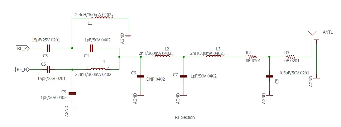
On my PCB, due to size restrictions, I have placed Balun & filter circuit along CC2640R2F IC. (I haven't seen this kind of placement in any document)

PCB size: 20mm x 20mm

PCB thickness: 0.4 mm

Copper Thickness : 35 um (micron)

I have referred PCB antenna design from swra117.pdf   (Small Size 2.4 GHz PCB antenna)

Desired range : ~50 feet. with 0dbm TX power. 

Following is the RF  section and Layout of my PCB. 

Please check whether this placement of Balun & Filter circuit and antenna will work or cause any issue. 

Note: On bottom side, GND poured except antenna section.  

Regards, 

Sharad

  • Hi Sharad,

    The layout of the balun and the RF match in itself looks very good. I do not like the unsymmetrical, relatively long, differential RF trace though. Also, your decoupling capacitors are not optimally placed. Since you are only using a few IO pins I would highly recommend using the 5x5 or the 4x4 QFN package to get more room around the CC2640.

    You should also consider using single ended RF with external bias.

    C6 is not required and can be removed. The antenna matching which is present in the schematic seems to be missing in the layout.

    Cheers,
    Fredrik
  • Hello Fredrik K,

    Thank you for your valuable comments.

    I have removed matching component section, because of limited space.
    But with this placement, can i get desired range?

    Thanks & regards,
    Sharad
  • Hi Sharad,

    50 feet should be achievable even with the deficiencies in the design.

    Cheers,
    Fredrik
  • Thank you Fredrik K.