This thread has been locked.

If you have a related question, please click the "Ask a related question" button in the top right corner. The newly created question will be automatically linked to this question.

TRF7970A: TRF7970A Integration with MSP430F6779A

Part Number: TRF7970A
Other Parts Discussed in Thread: MSP430F6779A,

Tool/software:

Hi Community,
we are integrating TRF7970A chip with MSP430F6779A controller for RFID project, as per datasheet for startup sequence I am following below steps:

    MOD_DIR_OUT;
	MOD_OFF;
	SLAVE_SELECT_PORT_SET;
	SLAVE_SELECT_HIGH;
	TRF_DISABLE;
	ENABLE_PORT_SET;
	MCU_delayMillisecond(6);
	TRF_ENABLE;
	SPI_setup();
	IRQ_PIN_SET;
	IRQ_EDGE_SET;
	IRQ_INT_ON;
	IRQ_CLR;

Here I am not enabling EN2 since we are using it in MODE 3 Half Power +3.3 VDC.
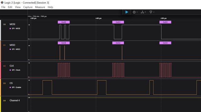
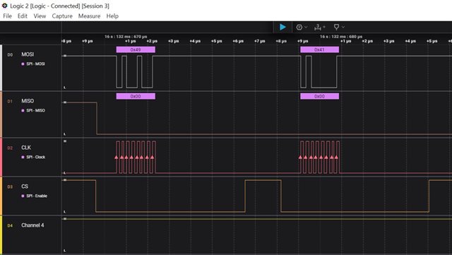
I am using SPI mode 0, with 4 MHz Data Clock Frequency, after TRF initialization I am giving these commands to keep TRF in IDLE state.

TRF79x0_directCommand(TRF79X0_SOFT_INIT_CMD);
MCU_delayMillisecond(4);
TRF79x0_directCommand(TRF79X0_IDLE_CMD);

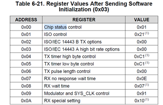
But upon checking the status of Chip status control register I am receiving only 0x00.
Please suggest me if I am missing anything.

Thanks and Regards 

Vishal Tyagi

  • Hi,

      Can you read out other registers? I want to isolate the problem if the register is zero or because of an problem on your SPI interface resulting in sampling a zero. The datasheet shows various registers reset values after a Software Initiation. If you are reading 0 on all the registers then there is something wrong on your SPI interface. Use a scope will be very handful to determine SPI issue. 

  • Hi Charles,

    Thank you for your response.

    During the TRF initialization process, I am observing activity on the MISO line, as shown in the attached screenshot:

    However, immediately after initialization, when issuing commands to read the Modulation Control Register and the ISO Control Register, no data is being received on the MISO line:

    Please share your observations that either the TRF is not being initialized correctly or there may be an issue with the SPI communication.

    Regards,

    Tyagi

  • Hi,

    Looking at your waveform, I think you want to read from addresses 0x9 and 0x1. Please follow the datasheet instructions to read a register in non-continuous mode. As you can see the first byte is "Addr x" and the next byte is the data. In your waveform, you are giving the "Addr x" and thinking that the data is returned on the same byte. Is that what you are trying to interpret? If this is the case then it is not true. In another word, to read a register, it is a two-byte operation with the first byte being the address to read from and the next byte is the returned data. As you can see in the below waveform, the SPI Enable needs to active across the two bytes. Maybe the problem is that you turn off the SPI Enable between the two bytes. Please refer to the datasheet for details.  

    Also to give a heads up, I will be out of office the entire net week, please expect delay in my response if you have further questions. 

  • Hi Charles,
    I understand that to receive the MISO byte, the master must generate additional clock cycles by sending a dummy byte along with the register address. I am now able to accurately capture the MISO data in variables:

    TRF79X0_ISO_CONTROL_REG = 0x21 (Correct as per Datasheet)
    TRF79X0_RX_WAIT_TIME_REG = 0x07 (Correct as per Datasheet)

    TRF79X0_RX_SPECIAL_SETTINGS_REG = 0x10. (Correct as per Datasheet)

    But for CHIP_STATUS control register still I am receiving data 0x00 only.

    During SPI probing, the data observed on the MISO line differs from the expected values. 

    Could you please clarify whether this discrepancy indicates invalid SPI data transmission or if the TRF79x0 is internally encoding/decoding the response before sending it over the MISO line.

    Thanks and Regards

    Vishal Tyagi

  • Hi,

      I'm currently on vacation for the entire week. I will reply your question when I have time later today. Please expect delayed response.

  • I understand that to receive the MISO byte, the master must generate additional clock cycles by sending a dummy byte along with the register address. I am now able to accurately capture the MISO data in variables:

    TRF79X0_ISO_CONTROL_REG = 0x21 (Correct as per Datasheet)
    TRF79X0_RX_WAIT_TIME_REG = 0x07 (Correct as per Datasheet)

    TRF79X0_RX_SPECIAL_SETTINGS_REG = 0x10. (Correct as per Datasheet)

    Glad that this is working. 

    During SPI probing, the data observed on the MISO line differs from the expected values. 

    As far as I can see on your above waveform, you are trying to write to address 0x08 (RX Wait Time register) with a value of 0x0. Next you are reading from 0x1 (ISO control register) which returns with a value of 0x10.