This thread has been locked.

If you have a related question, please click the "Ask a related question" button in the top right corner. The newly created question will be automatically linked to this question.

CC110L: Loop antenna questions

Part Number: CC110L


Tool/software:

Hello,

I'm working on migrating an old 869 MHz transmitter based on the ATA8403C TX chip to a CC110L-based design.

The ATA8403C uses a rectangular loop antenna, like this:


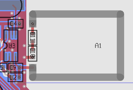
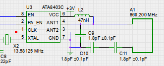
Loop dimensions: 18 x 13 mm.

As the CC110L has a balanced RF output, I'd like to use the same or similar loop antenna for the new design, also because it is really compact. Also, I understand that such a loop antenna is relatively immune to changes in capacitive loading due to environmental influences (e.g. someone holding the transmitter in their hand).

However, searching for CC110L + loop antenna turns up no circuit examples; every circuit example I can find employs a balun circuit, with a single-pole 50 Ohm antenna design.

Question: what filter circuit is advisable to connect the loop antenna to the CC110L RF_P and RF_N outputs? I understand that some filtering is necessary to avoid harmonics and keep in compliance with RF regulations.

Additional information: I am not exactly an RF guru, so my apologies if this question seems trivial to people with more knowledge on this subject matter. And oh, I have access to RF measuring equipment through a colleague of mine, so I can do some basic checking and tuning if necessary.

Thanks for any thoughts,

Richard

  • Hi Richard,

    Please see the discussion in the following thread:  CC1101: Balance Antenna 

    In short, we do not recommend using a balanced antenna for these designs and have not done any work on supporting them in many years because they are not the most practical solution in most cases (plus if you want a long range a loop antenna is probably not optimum for that application) - do you have an EDA tool available for simulation?

    You would need to simulate the TI reference design (including PCB parasitics) and then design a new differential filter/impedance matching circuit that targets the same load/source impedance(s) at the device pins. It's unfortunately normally not as simple as adding some filtering for passing performance. If designing a purely differential circuit this will also likely require at least as many components as the TI reference design.

    We would strongly recommend switching to the TI reference design (using an LC balun and filter/impedance circuit to a PCB or chip monopole antenna). For the least footprint possible you could also consider using an IPC (this increases the cost, however): https://www.ti.com/lit/swra250 

    Regards,

    Zack

  • Hello Zack,

    Thank you for your explanation and the links. No, I do not have EDA tools available for RF simulation. I use online impedance calculators for optimizing trace dimensions, and an actual (monopole) antenna is usually tuned by oversizing it and then trimming it back bit by bit.

    I was aware of the Johanson baluns - very neat devices, and pretty cheap nowadays as well, so I think I'll use one of those in the design.

  • Look into Yageo monopole antennas. seems like a fit for your application.
    au.mouser.com/.../

  • Hello Emil,

    Thank you, I'll certainly look into this - these chip antennas indeed appear to save a lot of space.