This thread has been locked.
If you have a related question, please click the "Ask a related question" button in the top right corner. The newly created question will be automatically linked to this question.
The data sheet for the CC1200 lists the optimum LNA input "differential input configuration" impedance as (apparently) 60 + j60. This would imply a "differential" input impedance of 60 - j60, which at 915MHz is 60 ohms in series with 2.9pF.
The "single ended configuration" optimum source drive is apparently 30 + j30. This implies an input impedance of 30 ohms in series with 5.8pF.
Unfortunately there are no schematic models of these impedances in the data sheet that would allow 100% certainty on what exact topology is meant by differential or single ended "configuration". For example, just using the real part, differential can mean 60 ohms between two differential input nodes. OR, it could mean 60 ohms to ground from each input node.
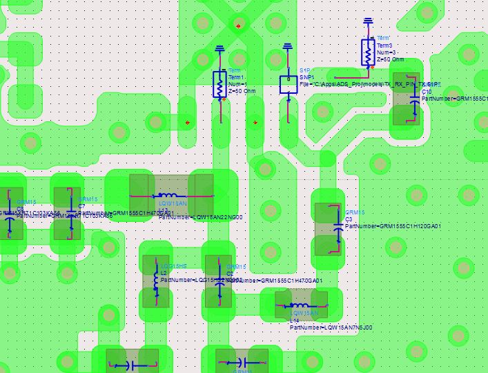
I note that the application circuit shows a lead-lag balun to the splitting from single ended drive to differential to drive the LNA inputs. There is no explanation of this circuit in any Texas Instruments materials I have been able to track down. But, using Z = 6.28 f L (classic formula for lead-lag balun inductor value), the L value of 12nH in each leg has impedance of 69 ohms. Thus, this seems to indicate an LNA input impedance on each of the plus and minus inputs of about 60 ohms to ground from each node (not 60 ohms between the nodes).
Is this the correct interpretation? The input impedance between each LNA input and GROUND at 915MHz is 60 ohms in series with 2.9pF?
Thanks, Farron
TER, I have another input here.
If the series model of single ended 30 - j30, or 30 ohms in series with 5.9pF at 915MHz, is transformed into a parallel mode model, it by coincidence transforms to 60 ohms in parallel with 2.7pF. That "60 ohms" has nothing to do with the "60 ohms differential" impedance in the data sheet. It is a resulting 60 ohms in parallel with 2.7 pF single ended equivalent model, where the 2.7pF is then resonated out as part of the balun circuitry.
That would be an approximately correct match with the circuitry shown for the balun in the 900MHz application circuit. I thus believe that balun circuitry is fundamentally OK. Also, it seems clear that the author of the data sheet is using the classic low frequency definition of differential impedance.
The data sheet would certainly be more clear if it both deemphasized the unused differential model in favor of the single ended model that the board designer actually uses, and gave clear definitions of both. It would also help if the apps materials described the series to parallel model conversion process, and how the balun is designed. Right now it is a mystery until the customer puts in quite a lot of time figuring it out.
Regards, Farron
TER, the user cannot simulate a match without being provided a model of the input impedance that he is matching to. Until he has the model, he has nothing to simulate with. That's why I am asking about the specific nature of the input impedance model.
If it were not practical to do single ended to differential conversion, then Texas Instruments would not be providing the CC1200 with a differential input that requires such a conversion. They show such a conversion on their 900 MHz application circuit.
The problems here are not simulation details or lack of practicality. They are:
1. The data sheet is emphasizing a differential input impedance which is really secondary to the single ended impedance that the user is really matching to. This misleads the user into thinking he needs to be working with the differential impedance in the simulations. No, the analysis and simulation on the part of the user starts with the single ended impedance.
2. No explanations are given in any applications materials that I have been able to find on:
A. The general need to convert the single ended serial input impedance model to parallel to design the balun and match it.
B. The design procedure of the balun. It is currently shown in the 900 MHz applications circuit without explanation of any kind.
What is needed here is an application note that spells it all out in detail. I've put the time in now to have figured it out, but this was a little tricky to get to the bottom of from the current state of the Texas Instruments collateral. If you want to discuss it in more detail, e-mail me at farron.dacus@yahoo.com, and I'll be glad to go into the full depth.
Regards, Farron
TER, that link appears to be dead, so I could not check it out.
The specification of optimum source impedance instead of load impedance is irrelevant, since the load impedance is simply the complex conjugate of the ideal source impedance. Thus, a 30 + j30 ideal source impedance can only mean a load impedance of 30 -j30. The reason the user prefers to work with load impedance is because his simulator usually drives from an ideal 50 ohm impedance. He usually prefers matching the load impedance, not the source impedance, because if the load is matched to be real then it can be driven from well controlled microstrip lines. The user cannot just drop that complex impedance on microstrip without mismatch and phase rotation over line length, so he needs to match it to real first.
To answer your question about why I am concerned about single ended load impedance, it is because the real board design IS single ended, and so is my s-parameter simulator. Each of the two drive points to the LNA inputs are by themselves single ended signals operating over ground plane, with a native impedance (depending on part and trace widths and height above ground plane) in the range of about 30 to 70 ohms (you cannot escape this when operating over a ground plane at 900 MHz over distances that are not negligible compared to a wavelength). From the matching point of view, it is a single ended circuit design problem.
Then, when the two equal magnitude 180 degree out of phase differential signals drive a differential input impedance, the signal balance generates a virtual ground at the mid-point of the differential impedance (this actually does happen on the emitters of the input differential pair). Thus, the load impedance seen by each of the driving sources is HALF the full differential impedance. The user MUST know this in order to set up proper matching, but no explanation of it is provided in the data sheet or apps materials. My suggestion would be to have a detailed app note written up on the subject (I could start one for you guys if you wanted).
So, what the user naturally wants to work with is single ended load impedance. At this point I am quite sure that single ended load impedance is 30 - j30 (under the condition of being correctly differentially driven to set up the virtual ground in the middle--what low frequency analog designers call a "half-circuit"). As a circuit model, that is 30 ohms in series with 5.9pF at 915MHz.
Now, that series model is perfectly valid, but it is easier to match if transformed to a parallel equivalent. A model of 60 ohms in parallel with 2.9pF has the same impedance over a narrow range around 915MHz. One side of this parallel R-C is connected to ground, and the other is the model of the LNA single ended input impedance. Try it on your s-parameter simulator and you will see the s11 looking into either model (series or parallel) is the same.
Now, an inductance of 10.4nH in parallel with that parallel input model will resonate off the 2.9pF and leave a single ended input impedance of 60 ohms. This is a convenient value to drive from the lead-lag balun, as the layout designer can set up matched lengths of 60 ohm microstrip from the balun outputs to the LNA inputs.
Regards, Farron
Hi TER:
Sorry to have to disagree, but the statement "The specification of optimum source impedance instead of load impedance is irrelevant, since the load impedance is simply the complex conjugate of the ideal source impedance" is not an assumption. It is first order linear circuit network theory as taught at the EE sophomore level. Linear network theory is applicable here for the LNA, since it is not driving into compression at the weak signal levels where good matching is needed.
Defining optimum source impedance instead of stating load impedance is of course also theoretically valid, but in my opinion it is less intuitive. It also suffers from the practical problem that the load must be matched to be real before going out on microstrip, so giving the load impedance is more in line with what students are taught and with what normally occurs in practice. I would recommend that TI adopt that approach in order to not confuse customers.
The reason I'm looking into it in such detail is that I am an RF design consultant who in 30 years in the RF design business has come to appreciate the high value of making sure I understand and apply correct fundamentals. I've witnessed several companies I worked for get those fundamentals wrong and lose millions of dollars, and sometimes go out of business as a result. In this specific case I am developing a high volume design for a client, where the link performance of the CC1200 alone is not adequate either as is or when supplemented with the CC1190 front-end. The custom low noise amplifier and a one watt power amplifier that have been designed for this app results in a system link budget about 12 dB better than the raw CC1200 and 6 dB better than the CC1200+CC1190. To get optimum performance, I can't throw away dB's in the matching from the off-chip LNA to the on-chip LNA, so I had to make sure I had that matching fundamentally correct. The matching shown in the CC1200 apps circuit is not bad, but it is not optimum either, and it was possible to improve it. By meticulously preserving every possible dB we now have a solid design that will meet the demanding requirements of this application.
Regards, Farron
TER:
I should allow for one additional possibility in the above. The "optimum" source impedance for the CC1200 Rx inputs might not be optimum power match (lowest reflection) but instead the match for minimum noise figure. The data sheet does not say, and since the noise figure is relatively high (again not given in the data sheet, but seems to be 7-8 dB based on sensitivity), I have been assuming it is more likely a power match. But, if it is a noise match, that at least explains the focus on optimum source impedance instead of simply giving the input impedances.
The confusion here has multiple sources, as follows:
1. Lack of definition of differential impedance and differential and single ended "configuration". These terms are used in the data sheet without clear definition, without discussion, and without illustrating figures.
2. General use of single ended circuitry in RF, even in the case of differential inputs, as microstrip is inherently single ended. This needs to be dealt with in advising the customer.
3. Optimum source impedance given without defining "optimum" (power or noise match).
4. Emphasis on simulation as an answer, instead of fundamental definitions and parameters as answers. Simulation discussions without prior definition tend to simply add confusion.
However, I do appreciate the effort made in trying to shed more light on the situation.
Regards, Farron