This thread has been locked.

If you have a related question, please click the "Ask a related question" button in the top right corner. The newly created question will be automatically linked to this question.

CC1310: AWR Receive Front-End Simulation

Part Number: CC1310

Hello,

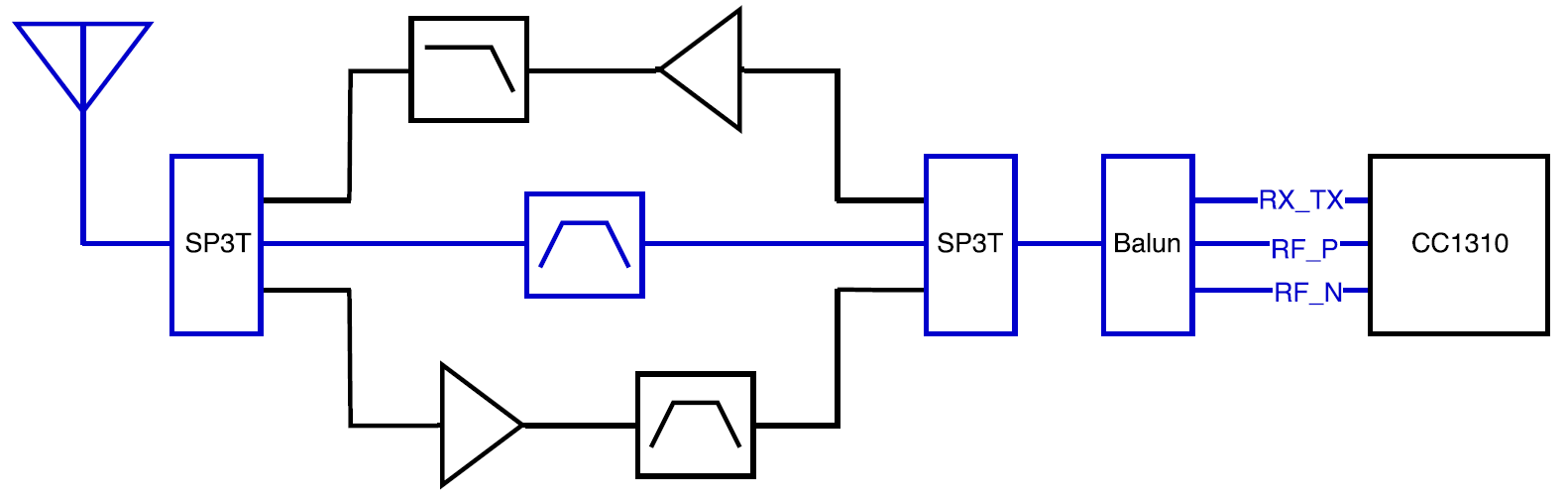
I am designing an RF front-end for the CC1310 using the 0850BM14E0016 balun and AFS14A26-915.00-T3 bandpass filter. Attached is the schematic of the receive chain and resulting S-Parameters plot. The touchstone files were imported into AWR and the MMCONV block was used to convert from differential to single-ended after the balun.

The port 2 impedance is set to ZS=44 + j15, as specified by the CC1310 datasheet. I am somewhat surprised that S22 is not at least below -10 dB. In fact, I was hoping to obtain somewhere around -13 to -15 dB at the very least.

Any thoughts on how to improve S22?

Thanks.

RX_Chain_Bypass_SCH.pdf

RX_Chain_Bypass_PLT.pdf

  • Not sure what you are trying to do.
    As stated in the datasheet, 44+j15 is the optimal differential impedance seen from the RF pins into the balun and filter. S-parameters are only valid for small signal. When in Tx, s-parameters are not valid since the voltage swings are large. The impedance is a tradeoff between what the PA want to see and what the LNA want to see. Having a low S22 would potentially make sense if you looked at a perfect match for a LNA but not for LNA + PA.

    But: 0850BM14E0016 provides the wanted impedance and provide a 50 ohm interface on the other side. The IPC contains balun + filter and you can connect an antenna to the output and pass regulations (www.ti.com/.../swra524a.pdf)

    If you want to design more filtering, simulate single ended from a 50 ohm point since the IPC has a 50 ohm port. Why do you plan to add a bandpass filter?
  • Hello,

    Thank you for the response. I believe that I am evaluating small-signal, as I am looking at the RX bypass chain (see below). The AWR model that I made is basically everything in blue.

    You will notice that I estimate the insertion loss of the RF switches to be around 0.25 dB in the model. Also, I convert the RF_N/RF_P differential combination to single-ended using AWRs MMCONV. At port 2, I am looking for the 44 + j15 impedance. Port 1, where the antenna is, is set to 50 ohm.

    Based on the fact that the 44 + j15 impedance is optimized for both the internal LNA and PA of the CC1310, it now makes sense that S22 is not as good. I guess I shouldn't worry about it, as the IPC is matched properly. Instead, I have now set port 2 to 50 ohms prior to the balun. Attached are the updated schematic and plot, which both look just fine.

    Since the IPC already contains a filter, do you think I should get rid of the bandpass filter in the bypass chain? Maybe even the external LNA?

    6012.RX_Chain_Bypass_SCH.pdf

    8640.RX_Chain_Bypass_PLT.pdf

  • The app note I linked to shows how much the IPC filters. If the filtering is not sufficient for your use you can add extra filtering but a LP filter would probably be sufficient. And as I wrote you can design this with 50 ohm in, 50 ohm out since the single ended port on the IPC is 50 ohm.

    Just curious on the block schematic: Why do you use 3 different paths? Why not use a FEM with PA and LNA and backoff the power if you want to be under 14 dBm?
  • Thanks for the app note.

    There are a couple reasons I am not using a FEM. I am a university student and would like to acquire more RF experience, so research, impedance matching, and simulation are all valuable skills to know. From a functional standpoint, the LNA I selected has much higher gain and low NF compared to most FEMs, and my PA can go up to 30 dBm (the FCC limit). With the bypass path I can turn off the LNA and PA to save power, and also avoid the low PA efficiency at reduced input power.

  • Ok, makes sense.