This thread has been locked.

If you have a related question, please click the "Ask a related question" button in the top right corner. The newly created question will be automatically linked to this question.

CC1101: RF chip (CC1101) with Blind area in Receiving range less than 5m

Part Number: CC1101

in our recent production (Alarm Clock Receiver), we found many RF chips CC1101 with a serious defect (there is a Receiving Blind area in receiving range less than 5m) , the defect rate is near to 8%, in this Blind area, the receiver almost can't respond our transmitters except for the occasional response.

Alarm clock Receiver description: Carirrer Frequency: 433.92MHz, Modualation: OOK, Baud rate: 333.34bit/s, Frame format: a reference(1/3bit length)+12information bits+back-off (12bits of length).

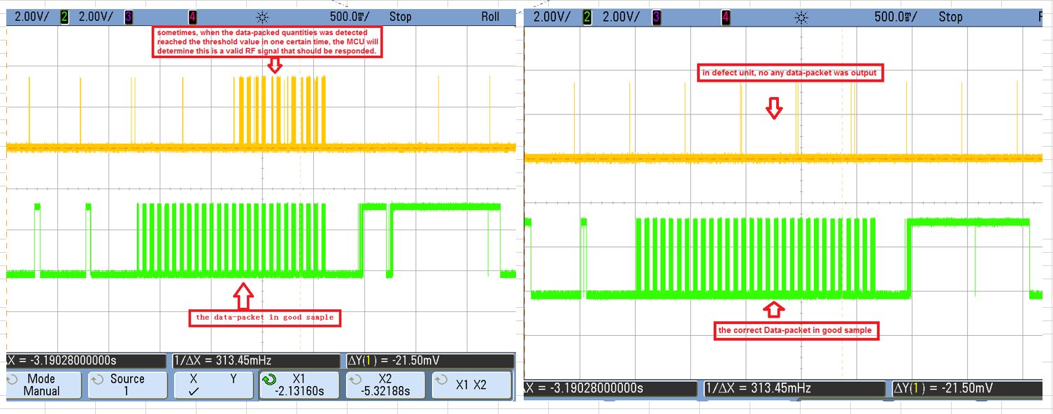
we test the RF chip GDO0 pin, we found the signal data frame in defect sample is incorrect or incomplete compared with the good samples, details see below photos,

now, we already holded the  production, we don't know what happened in CC1101 inner, Dear TI technicans, please help to check and analyze to find the root cause and advise your solution for our product, 

if you need more information, please inform us, thanks.

                                                                                                              YKLi.

  • I would assume that 

    http://www.ti.com/lit/pdf/swra147

     covers what you are seeing. 

  • Dear TI technican,

    after checked the Design Note DN010 that you sent to me, you think maybe "the saturation limit of approximately -15dBm" is the root cause to impact RF performance in our product, and you recommended two solutions for our reference in both of transmitter and Receiver side.

    then, follow up your suggestion, i did some test as below for your reference,

    1) for those defect units with "Blind area" in less than 5m range, if we put the transmitter very near to Receiver, for example, 20cm -30cm, the RF performance is very stability, i did the test more than 20times, every test is successful. but, when put the transmitter in other test point in 5m range, the "Blind area" was present, after remove the transmitter out of "Blind area", the RF performance is also stability.

    2) i decrease the radio power -20dBm in reference transmitter, and did the same test in item1 above, the test result is the same as item1.

    based on the test result on above item1 and 2, it seems that the root cause seems not be" the saturation limit".

    more information for your reference as below,

    1) this is our existing product, already be produced over 8years, in past time, only seldom of complaints just like it from our customers, but, for our recent PO, the defect rate (poor RF performance in short range) is near to 8%.

    2) i had try to mount the defect CC1101 on our 868 Receiver and did the RF receiving test, i also can found there are many "Blind point" in range of 15m - 160m compared to those good samples, compared to the 433 Receiver, the "Blind point/area" in 868 Receiver seems to be in more long area.

    I  am very appreciate your quick reply, thanks.

  • - Which RSSI do you have when you have have good reception vs poor reception?

    - Is what you see dependent on frequency? You could try to go a few MHz up/ down and see if you see a difference.

    - Do you see any difference if you move the receiver to a different location and repeat the test? 

    - Do I understand you correctly: If you place a failing board and test this and replace it with a good board the results will always be the same even if you repeat the test?

    - Would you be able to do a PER vs level measurement? Ideally you would need a signal generator for this and the test should be done conducted (not over the air). Send 100 packets for each step and see if you get a lot of failures for some input levels. I believe we have had cases where the chip has been partly ESD damaged in the way that damage some of the gain steps in the AGC. If that is the case you will see poor performance for given gain stages.  

  • Hello TI technicans,

    about your questions, please see YK's answer in Green below

    - Which RSSI do you have when you have have good reception vs poor reception?

    YK: we are trying to test, but, no test result at present.

    - Is what you see dependent on frequency? You could try to go a few MHz up/ down and see if you see a difference.

    YK: the Centre frequency is 433.92MHz for our products, i did many test to change the centre frequency from+/-5KHz to +/-60KHz, in this wide carrier frequency, the defect units is still "Blind area" in range less than 5m, for those good units, they are still good performance without "Blind area".

    - Do you see any difference if you move the receiver to a different location and repeat the test? 

    YK: we did many test in different location, for example, our office, one small open field and a wide open field, the test result is the same, the defect units is still with "Blind area" in different test location, but for good units, they are still ok.

    - Do I understand you correctly: If you place a failing board and test this and replace it with a good board the results will always be the same even if you repeat the test?

    YK: Just for your understanding better, i describe the defect RF chip as below, if we use a good RF chip to replace the defect RF chip in one defect unit, the defect unit will change good, vice-verse, if we mount one defect RF chip in one good unit, the RF performance in good unit will change bad.

    - Would you be able to do a PER vs level measurement? Ideally you would need a signal generator for this and the test should be done conducted (not over the air). Send 100 packets for each step and see if you get a lot of failures for some input levels. I believe we have had cases where the chip has been partly ESD damaged in the way that damage some of the gain steps in the AGC. If that is the case you will see poor performance for given gain stages.  

    YK: we did the "PER vs level" test  according to your suggestion (through cable, not over the air), the summary is below, 

    1) when RF Level less than -100dBm, RF GDO0 output is abnormal in both of defect unit and good unit, 

    2) in range from -100dBm to 20dBm, the GDO0 output is normal in good unit.

    3) in range -100dBm to -95dBm, the GDO0 output is abnormal in defect unit. (YK: in my opinion, maybe this is a tolerance in different RF chip).

    4) in range from -95dBm to -69dBm, the GDO0 output is normal in defect unit.

    5) in range from -69dBm to -50dBm, the GDO0 output change bad in defect unit.

    6) in range from -50dBm to 20dBm, the GDO0 output change good in defect unit.

    Test result: we can see when RF signal is in range -69dBM to -50dBm, there is a obvious "Blind area" in defect unit.


    YK: about your deeply analysis result that maybe some ESD parts was demaged inner RF chip, to lead one error step gain control in AGC, in my opinion, i think this may be a reasonable guess, however, Bellman company need a real root cause that test and verified by TI, at present, we already held the production over 2weeks due to this case, would you like to test and find the root cause by testing the defect RF chips? if yes, i can send some defect RF chips to you, thanks very much.