We are in development of a new design utilizing the WL1805MOD. During the initial prototype build, we are encountering solder voiding on some of the inner ground pads of between 40-60%.
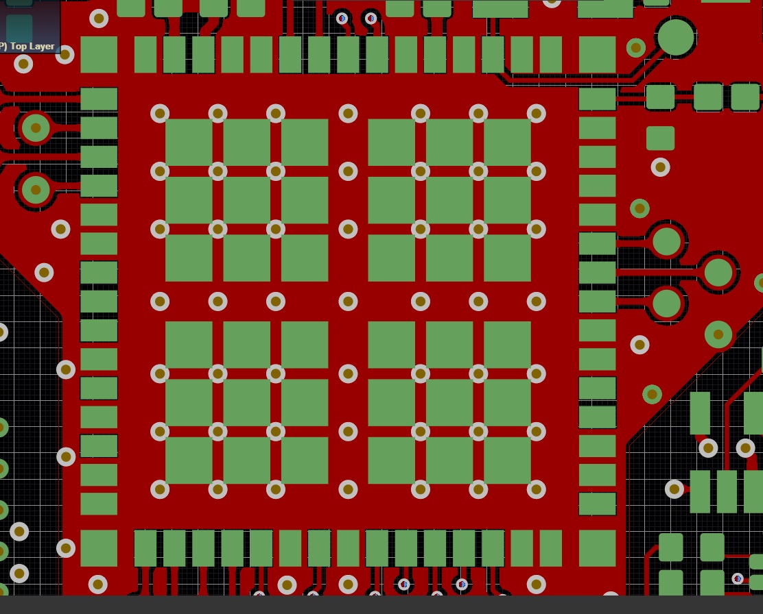
We are using the pad size and mask opening shown in section 9 of the datasheet. Per the layout recommendation of section 7, we have a copper pour on layer 1 under the component, connecting all the ground pads:

We left the mask opening and stencil per the footprint, such that the inner ground pads were essentially solder mask defined pads over the single copper pour. The via pattern is per the recommendation in section 7.
The CM was unable to fix the voiding by tweaking the reflow profile. Their recommendation is to use large inner pads, where the center 4 blue areas shown above would each be mask defined pads. Was that the intent of the illustration shown in the datasheet? Does TI have any recommendations to reduce solder voiding?