Because of the Thanksgiving holiday in the U.S., TI E2E™ design support forum responses may be delayed from November 25 through December 2. Thank you for your patience.

This thread has been locked.

If you have a related question, please click the "Ask a related question" button in the top right corner. The newly created question will be automatically linked to this question.

Problem on photodiode amplifier circuit

Other Parts Discussed in Thread: OPT101

Hello guys, 

I've working on a simple circuit which is trying to measure the output of a regular photodiode ( OSRAM BPW34-FA PHOTODIODE, IR FILTERED). 

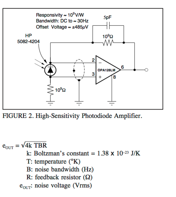
And the circuit I'm using is shown above from www.ti.com/.../sboa061.pdf

I don't really know what the dot circle mean so I ignore it. 


Could anyone explain to me about this circuit? Because as I know, the -IN and +IN of the amplifier should have the same voltage. But from what I measured, they are different. Although the output doesn't change according to the light intensity, I don't understand how this circuit works.

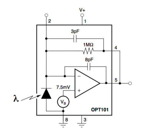
And further more, while I was trying to understand the circuit, I compare this circuit to an inner circuit of another amplified photodiode (OPT101). www.farnell.com/.../682873.pdf

These two circuit are pretty similar, besides the voltage across the photodiode on the one above is fixed by around 7.5mV and the output of the inner photodiode is amplified by the current produced multiplying the resistor. 

Could anyone tell me the difference between these two circuit ?  Thank you. 

  • Hi Tzu,

    Let's start with the "dot circle"; this means if the photodiode is mounted remotely you must use shielded cable to connect the PD to the opamp. In the data sheet you referenced you can see they went one step further and also suggest connecting the metal shell of the photodiode (if it has one) to the shield as well. If you're not mounting the PD remotely you can ignore this.

    There's a couple of things to know about this circuit. You are dealing with some very "small" currents here. Having worked with photodiodes, large area P-N "plates" and photomultipliers I've learned a lesson (or three). Layout is critical in these applications; your PCB layout is critical, as is how the devices are mounted. The resistors shown are so high impedance you can "blow" on the circuit and see changes in the output. The PCB must be very clean so as to not cause offsets, etc. You must use good decoupling on the power supply pins; this is a case where in addition to the 0.1µF ceramic caps used at the power pins, I'd also use a 10µF Tantalum capacitor in parallel with the 0.1µF ceramic. Again, this must be at the power pins; there should be almost no trace (allow for soldermask) between the pin and the caps. In the "old days" we would go so far as to mount the resistors and feedback cap on Teflon standoffs.

    All of the above is geared towards "instrumentation" design; what are you actually measuring? You mention that you don't see any change in the output. The photodiode you've chosen has a "daylight filter" to filter out "visible light" more or less. This device is designed to be used with infrared light; as such, you'll need an IR source to see any appreciable change in the output. If you substitute a PD without the filter you should see great variations in the output signal with changing light levels.

    The OPT101 is virtually the same as the circuit above it in a monolithic design; everything needed is on the device. As stated in the data sheet, this topology eliminates many of the errors and issues that come up when using discrete components. It also does not have a filter so will be responsive to "white light" (refer to the curves in the datasheet), however, as you can see it is also mostly responsive in the IR region as well.

    Again, what is your application? There may simpler ways to achieve what you're after.

    Mike T.