This thread has been locked.

If you have a related question, please click the "Ask a related question" button in the top right corner. The newly created question will be automatically linked to this question.

watchdog fail count count does not decrement

Other Parts Discussed in Thread: TMS570LS20216

Hi,

This is in continuation of my previous post in PMIC forum, 

e2e.ti.com/.../1784793

I’ve run the watchdog function in diagnostic state but the watchdog fail count hasn't come down to 0.

The WD_FAIL_CNT has this sequence: 67777777776777777777

Do you have any idea on why this problem may happen?

Thanks,

Fatemeh

  • Hi Fatemeh,

    You are not "feeding" the WD correctly.  Thus the WD_FAIL_CNT is not decrementing properly.  Are you using trigger mode or Q&A mode?

    You have to align the MCU timer for the WD to the TPS65381 watchdog clock, call synchronization.  The easiest way to do this is to write to WDT_WIN1_CFG or WDT_WIN2_CFG registers.  Doing so will update the programmed time for that specific window (unless the data written is the same as in the register) and the key is it will re-start the WD with a new WD sequence (WIN1 + WIN2).  This is when the timer in the MCU for the WD should start. 

    In the case you are using trigger mode you should:

    • Make sure you have configured WDT_WIN1_CFG and WDT_WIN2_CFG to the times needed for your application.  We recommend using at least 2 (decimal) in these settings. 
    • Target the trigger to be in the middle of the WINDOW 2 for the programmed times of WIN1 + WIN2. The external trigger pules from the MCU has to be at least high for 32us to pass the deglitch on WDI/ERROR pin. 
    • Once the TPS65381 has detected the trigger pulse it will start a new WD sequence (WIN1+WIN2), the MCU should start a new sequence as well.
    • See section 5.4.1.13 in the DS.

    In the case you are using Q&A mode:

    • Make sure you have configured WDT_WIN1_CFG and WDT_WIN2_CFG to the times needed for your application.  We recommend using at least 2 (decimal) in these settings. 
    • Make sure you are answering the correct question (WDT_TOKEN_VALUE)
    • The first 3 ANSWERS (RESP3, 2, 1) should be in WINDOW 1 and the final, fourth ANSWER (RESP0) should be in the first half of WIN2 based on programmed times of WIN1 and WIN2. 
    • See section 5.4.1.14 in the DS.

    You may want to start with WDT_WINx_CFG settings much higher to get the software flow down then lower them to make the timing faster.  Using longer times to develop the software will allow you to monitor what the MCU is doing better.

    You may also use (poll) the WD_STATUS register to see the status flags which may help you debug what you are doing wrong to the WD (ie to fast, to slow or wrong answers).

    Please note below are a few clarifications on the timing of the watchdog that may help that are in work for an update to the datasheet to clarify it. WINDOW time calculations where RW[6:0]  bits in WDT_WIN1_CFG and RW[4:0]  bits in WDT_WIN2_CFG.

    Trigger Mode: WINDOW1 = CLOSE and WINDOW2 = OPEN

    Q&A Mode: WINDOW1 = OPEN and WINDOW2 = CLOSE

    Due to the unknown timing it is recommended to use settings for WINDOW 1 and WINDOW 2 of two or higher. WINDOW 2 could be set as low as 1, but the response from the MCU should be targeted to the mid point or less of the ideal WINDOW 2 time.

    • tWIN1_MIN = (RT[6:0] - 1) × 0.55 × 0.95 ms
    • tWIN1_MAX = (RT [6:0]) × 0.55 × 1.05 ms
    • tWIN1_IDEAL = (RT [6:0]) × 0.55

    • tWIN2_MIN = (RW[4:0]) × 0.55 × 0.95 ms
    • tWIN2_MAX = (RW[4:0] + 1) × 0.55 × 1.05 ms
    • tWIN2_IDEAL = (RW[4:0] + 1) × 0.55

    • tSEQUENCE_MIN = (tWIN1_IDEAL + tWIN2_IDEAL – 0.55 ) *0.95
    • tSEQUENCE_MAX = (tWIN1_IDEAL + tWIN2_IDEAL) *1.05

    Thus the "known" times where ANSWERs or TRIGGER should be targeted are:

    • tWIN1_KNOWN_MIN = 0
    • tWIN1_KNOWN_MAX = tWIN1_MIN

    • tWIN2_KNOWN_MIN = tWIN1_MAX
    • tWIN1_KNOWN_MAX = tSEQUENCE_MAX

    If no response is provided TIMEOUT will occur:

    • tTIMEOUT_MIN = tSEQUENCE_MIN
    • tTIMEOUT_MAX = tSEQUENCE_MAX

    Regards,

    Scott

  • Hi Scott,

    The WD has been configured in Q&A mode.

    As you said “start with WDT_WINx_CFG settings much higher to get the software flow down then…” I increased the WDT_WIN1_CFG and saw that by setting this to 400 or higher, it made the WD_FAIL_CNT be decremented to 0 but could I do this change?

    My code is copy from the CCS_RM46_NoRTOS project. This is part of the code used in configuring the WD windows

    unsigned short OPEN_WINDOW_CONFIG = 500, CLOSE_WINDOW_CONFIG = 15;

    ecmpWdgWindowConfig(OPEN_WINDOW_CONFIG, CLOSE_WINDOW_CONFIG);

    --------------------------------------------------

    void ecmpWdgWindowConfig(unsigned short OPEN_WINDOW_CONFIG, unsigned short CLOSE_WINDOW_CONFIG)

    {

    ecmpIfSetRegister(ECMP_WDG_OPEN_WINDOW_CONFIG, (unsigned short) (OPEN_WINDOW_CONFIG/0.55));

    ecmpIfSetRegister(ECMP_WDG_CLOSE_WINDOW_CONFIG, (unsigned short) (CLOSE_WINDOW_CONFIG/0.55) - 1);

    while (ecmpIfGetBit(ECMP_WDG_STATUS, 2) == 1);

    }

    -------------------------------------------------

        TrgPulseOpen = OPEN_WINDOW_CONFIG*1000/2;

        TrgPulseClose = OPEN_WINDOW_CONFIG*1000/2+CLOSE_WINDOW_CONFIG*1000/3;

        rtiREG1->CMP[2U].COMPx = TrgPulseOpen;//write to the open window in the middle of Topen

        rtiREG1->CMP[2U].UDCPx = TrgPulseClose;//write to the close window at 1/3 of Tclose

    Thank you very much,

    Fatemeh

  • Hi Fatemeh,

    I recommended setting the WD windows longer to make them easier for the software to achieve and then you can shorten back up once the software flow is working correctly. I do not support the TMS570 MCU and have never used their software, however many customers have used the Q&A WD with their software library with no issues so I assume there is a configuration or software use issue in how you are using it.  You could post questions about the software to their forum. I can help support them if necessary in your use case of their software.  

    The first thing I noticed is you cannot set the WD to 400 on the TPS65381.  You may think you have done so, but this is not a valid configuration, you need to read back RD_WIN1_CFG and RD_WIN2_CFG to know what window settings are actually set on the TPS65381. 

    The maximum for WINDOW 1 is 127 decimal (0x7F hex) and maximum for WINDOW 2 is 31 decimal (0x1F hex).  With these settings in WDT_WIN1_CFG and  WDT_WIN2_CFG registers the equivalent window times would be calculated below:

    Time (ms) from WD Sequence start
    WINDOW1 WIN1min 65.84
    WIN1max 73.34
    WIN1ideal 69.85
    WINDOW 2 WIN2min 16.20
    WIN2max 18.48
    WIN2ideal 17.60
    WD Sequence SEQUENCEmin 82.56
    SEQUENCEmax 91.25
    TIMEOUT TIMEOUTmin 82.56
    TIMEOUTmax 91.25

    With such a setting the responses should look like:

    KNOWN "VALID" RESPONSE TIME Time (ms) from WD Sequence start Trigger Mode Q&A Mode
    Response Target for WIN1 WIN1_KNOWN_MIN 0.00 Do not trigger in WIN1 KNOWN time RESP3, 2, 1 should be in this range
    WIN1_KNOWN_MID 32.92
    WIN1_KNOWN_MAX 65.84
    Response Target for WIN2 WIN2_KNOWN_MIN 73.34 Trigger in WIN2 KNOWN time RESP0 must be in this range
    WIN2_KNOWN_MID 77.95
    WIN2_KNOWN_MAX 82.56

    To ensure the ANSWERs would be counted correctly RESP 0 has to be in WINDOW 2's known valid time, which in this case is between 73.34ms and 82.56ms from the start of the WD sequence.  A new WD sequence is started in a few ways:  WR_WDT_WINx_CFG, TIMEOUT event where 4 WD ANSWERS were not given before the end of the WD Sequence (TIMEOUT flag sets), and the 4th ANSWER given within a WD Sequence (doesn't matter if they ANSWERs are correct or not) on the 4th ANSWER the WD Sequence will restart.  The MCU needs to re-sync it's WD clock to line up with the new WD sequence to make sure RESP0 is in WIN2.

    For the real application the timing of the WD needs to be set such that the MCU will be RESET by the TPS65381 in the necessary time allowed by the specific application. If you use the WD and decrement it all the way to 0 with good ANSWERs it will take 5 bad events until ENDRV will be forced low and 8 bad events until NRES will be forced low if WD_RST_EN is set, the longest a single bad event can be is TIMEOUT maximum.  Some applications use the WD by keeping the WD_FAIL_CNT between 2 and 3 or 3 and 4 so that only one or two bad events is needed to cause a system impact.  This way the software also confirms the TPS65381 WD is also still working by having a good then bad detection from the MCU. 

    A more typical example is something like WIN1 = 0x23h and WIN2 = 0x06h

    Time (ms) from WD Sequence start
    WINDOW1 WIN1min 17.77
    WIN1max 20.21
    WIN1ideal 19.25
    WINDOW 2 WIN2min 3.14
    WIN2max 4.04
    WIN2ideal 3.85
    WD Sequence SEQUENCEmin 21.42
    SEQUENCEmax 23.68
    TIMEOUT TIMEOUTmin 21.42
    TIMEOUTmax 23.68
    KNOWN "VALID" RESPONSE TIME Time (ms) from WD Sequence start Trigger Mode Q&A Mode
    Response Target for WIN1 WIN1_KNOWN_MIN 0.00 Do not trigger in WIN1 KNOWN time RESP3, 2, 1 should be in this range
    WIN1_KNOWN_MID 8.88
    WIN1_KNOWN_MAX 17.77
    Response Target for WIN2 WIN2_KNOWN_MIN 20.21 Trigger in WIN2 KNOWN time RESP0 should be in this range
    WIN2_KNOWN_MID 20.82
    WIN2_KNOWN_MAX 21.42

    You also need to make sure for each WD sequence you calculating the ANSWERs to the question for that sequence.  The TPS65381 will generate a new question after every correctly answered sequence so the MCU must calculate the ANSWERs to go with the new question.

    Scott

  • Scott,
    I appreciate your time answering my question.
    The current design has some flaws that fails when using the power IC.
    When there is no problem in the hardware I’ll continue this post.

    Thanks again,
    Fatemeh
  • Hi Scott,

    Sorry for responding with delay, it is because of the holiday and also solving the last problem.

    Now I could serve the watchdog correctly. The WD-fail-count had decremented to zero but when I have powered the board off and again have made it on the TPS went to the safe state and I couldn’t reprogram the micro. By disconnecting the NRES pin of the PMIC and the POR_RESET (cold reset) of the micro this problem has been solved too.

    I put the TPS in active state after the WD-fail-count reached to zero, so the WD-fail-count initialized to 5 and being started to decrement. I also set the EN_DRV to 1 when in active mode the WD-fail-count again reached to zero. Then

    I wanted to inject an error and see what will happen, would it go to the safe state or not?

    I programed the micro with the code that would inject an error in its dual cores and the ERROR pin of the micro went “high” also the ERROR pin of the TPS.

    Now the NRES is high and ENDRV pin is low and unfortunately I just counter the same old problem again in connecting to micro.

    The DS stated that “When improper MCU operation is detected, the ENDRV pin is pulled low to disable the safing path or external power stages.” Is it required to place a pull up resistor and a switch between the ENDRV pin of TPS and micro? So do you think if we pull the ENDRV pin high, could solve our problem?

    I don’t know what the error injection does that made problem in TPS. I guess the VCCIO does not reaching to 3.3V, it is lower than that, about 3.1, but I am not sure about it!

    I would appreciate if you would tell me your opinion about this problem.

    Thanks again,

    Fatemeh

  • Hi Fatemeh,

    You need to keep in mind the TPS65381 has real time monitoring functions on it and if conditions are not met during software debug the device may do actions it is designed for in the state machine and monitoring functions.

    How have you configured the MCU ESM block on TPS65381?  Do you have SPI datalogs showing which state the TPS65381 is in during these events (FSM[2:0] bits in SAFETY_STAT_5 register? 

    ENDRV pin has an internal pull up within TPS65381, if you have overloaded that pull up externally then a suitable external pull up will be necessary. This is the safing output and as long as the MCU is not an Output pushing high (which is not an acceptable h/w design, but rather a high impedance input you shouldn't need a switch).  Normally the MCU only independently monitors the ENDRV signal or shouldn't directly see it.  There are normally parallel paths into the output stages, ENDRV and one or more from the MCU or other peripherals that all need to be "good" for the output stages to be able to be used.

    The MCU error output should be connected to the ERROR/WDI pin.  This is the MCU ESM error input.  MCU ESM should only be used when the watchdog is in Q&A mode. 

    Can you clarify the statement: " I guess the VCCIO does not reaching to 3.3V, it is lower than that, about 3.1, but I am not sure about it!"   What  is VCCIO?

    Additional question: when you created this MCU error what does the MCU do?  If it stops send watchdog commands and you have enabled reset via watchdog with the WD_RST_EN bit then when the WD times out the TPS65381 will RESET and not stay in SAFE state.

    Scott 


  • Scott,

    I’ll try to explain my observations clearly and hope not to confuse you.

    I wrote a program to set up the TPS in Q&A mode and run the WD on it. In this program first I put TPS in diagnostic state and ran the WD in this mode. WD was working correctly and when it decremented to zero I set the DIAG_EXIT bit to exit from diagnostic state hence it went to the active state. The WD_FAIL_CNT was initialized to 5 and being started to decrement. When WD_FAIL_CNT reached to zero I set the WD_RST_EN bit to 1 and then I’ll check it, if WD_RST_EN bit was zero I do an action.

    The TPS has been in active state; if I reprogramed the MCU again, TPS was in active state from the first. I don’t know why it is in active state from the first; I mean why it keeps the last state? Does it have any memory to keep the TPS states?

    How have you configured the MCU ESM block on TPS65381?  Do you have SPI datalogs showing which state the TPS65381 is in during these events (FSM[2:0] bits in SAFETY_STAT_5 register? 

    If I understand your question correctly, I don’t have any SPI data logs and I can’t connect to the IDE to see this register but I’ll say that TPS should be in active state, I mean the last state that it was there.


    I erase the MCU flash from the previous program that serves WD in Q&A mode. After that in another program I did an error injection and wanted to see what will happen. It is a separate program from the program for setting up the TPS. I ran this program before when there is no Power IC (TPS). And at that time there is no problem. I’ll explain the operation of this error injection program.

    In this program, first the LED on the board is starting to flash quickly for 20 times, and then error is injected in the MCU’s dual cores. If the MCU can detect the error then the ERROR pin will be high and one flag will be set. The program checks this flag and if it become set then the LED will start to flash slowly for 10 times and I will know that the error has been detected.

    This was the operation of my error injection program.

    And now the situation is:

    1. The LEDs are flashing quickly
    2. The ERROR pin of the MCU is high.
    3. I have disconnected the RESET pins of TPS and the micro from each other, so TPS can’t reset the micro.
    4. I also have disconnected the ERROR pins of TPS and the micro, so the error on MCU can’t transfer to the TPS and in case of an error in the MCU the ERROR/WDI pin of TPS will not be high, it will remain zero.
    5. Can you clarify the statement: " I guess the VCCIO does not reaching to 3.3V, it is lower than that, about 3.1, but I am not sure about it!"   What is VCCIO? I mean the VDD3.5 is not produced correctly. It must be 3.3V that is connected to VCCIO of the micro but it is fluctuating around 3V, it is not reaching to 3.3V also the reset pins of both TPS and micro have the same situations. VCC and VCCIO are two Supply Voltages for MCU core and its IO respectively that come from TPS. In order to work properly, VCC must be 1.5V and VCCIO must be 3.3V but they are below than 1.5V and 3.3V and have fluctuations.
    6. When I force rest the micro by connecting its reset pin to the ground I see that all voltages are produced correctly, I mean when MCU is not working and its ERROR pin is low, TPS make the VDD3.5 correctly and its NRES pin is fixed to 3.3. But I disconnected the ERROR pins of each other so what is the reason that TPS hasn’t produced the VDD3.5 correctly?
    7. I don’t know why the LED is flashing quickly if the error be detected I wrote in the program to make the LED to flash slowly. It is likely that one thing in this program prevent TPS to produce voltages needed for the MCU, so the MCU Voltage Monitoring system internally reset the micro. Hence the MCU is always in reset and the first of my program always is running. (I mean the LED is blinking quickly). Is right!?
    8. In no way I could connect to the micro through my IDE.

    Sorry, I don’t understand what you are saying here. “You need to keep in mind the TPS65381 has real time monitoring functions on it and if conditions are not met during software debug the device may do actions it is designed for in the state machine and monitoring functions.

    Unfortunately, I hardly could understand your explanations. Would you please explain it in a simple way that I could understand the meaning of your sentence? Sorry again for saying this, it is because of my poor English language knowledge.

    Thank you very much for your assistance,

    Fatemeh

  • Scott,

    I noticed a new issue which resolves some of the ambiguities.

    Please wait for my next post.

    Thanks

    Fatemeh

  • Hello Scott,

    I think I could setup the TPS as a power IC for the MCU correctly; this is of course with your help. But something has remained unclear to me.

    In connection to my previous posts, I noticed that the reason of resetting the MCU was not the error injection process in any way. As I told before, in my error injection program, at first the LED on the board is starting to flash quickly for 20 times, and then error is injected.

    The ERROR pin must become low in case of existence of any error, but this pin was always high. In addition when we had disconnected the ERROR pin of TPS and MCU of each other, the situation was remained unchanged so this has implied that the problem was not due to the error injection process. Just one thing has been remained and it was the command for blinking the LED.

    so I want to know:

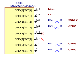
    1. The reason for resetting the micro when I use the blink command to flash the LED in the MCU; In addition to that, I ran this program before, when the micro’s power was not provided from the TPS, I mean when there was no TPS on the board. This instruction in CCS

    gioToggleBit(gioPORTA, 0); 

    means to toggle Bit0 of GIO PortA. It is the pin 118 of TMS570LS20216 shown as (GIOA[0]/INT[0]) in its Pinout Top View.

    This pin is connected to the LED on the board. I don’t know why toggling this pin make TPS to disconnect the voltage reaching to the MCU. I don’t know how they relate to each other?

    This is a pieces of the design that show the GIO pin connections,

    2. And the other question is the operation of ENDRV: I think a switch is needed for this pin between TPS and the micro, but I don’t have any prof to this. I think sometimes disconnecting this pin solved the problem of connecting to the micro.

    Thanks to your help,

    Fatemeh

  • Hi Fetemeh,


    You wrote:


    S5. Can you clarify the statement: " I guess the VCCIO does not reaching to 3.3V, it is lower than that, about 3.1, but I am not sure about it!"   What is VCCIO? I mean the VDD3.5 is not produced correctly. It must be 3.3V that is connected to VCCIO of the micro but it is fluctuating around 3V, it is not reaching to 3.3V also the reset pins of both TPS and micro have the same situations. VCC and VCCIO are two Supply Voltages for MCU core and its IO respectively that come from TPS. In order to work properly, VCC must be 1.5V and VCCIO must be 3.3V but they are below than 1.5V and 3.3V and have fluctuations.


    --> A5: If VDD3/5 and VDD1 are not regulating stably then there is a major issue.  The first thing to check is are you overloading these regulators beyond their current limits?  If the rails hit current limit the voltage will start to drop.  If the MCU does not have a stable voltage supply within it's specified operating range then operation is not guaranteed for the MCU. RESET line is pulled to up VDDIO on the TPS65381 so if VDDIO fluctuates, then so will nRES.  You also wrote in another e-mail about high temps, the device could be also hitting thermal limits.  Have you analyzed the load currents and thermal design of your PCB to make sure you keep both of those in spec for all the rails and the VDD6 pre-regulator at the top level?  Statement 6 makes me believe the MCU is overloading the regulators.


    S6. When I force rest the micro by connecting its reset pin to the ground I see that all voltages are produced correctly, I mean when MCU is not working and its ERROR pin is low, TPS make the VDD3.5 correctly and its NRES pin is fixed to 3.3. But I disconnected the ERROR pins of each other so what is the reason that TPS hasn’t produced the VDD3.5 correctly?


    --> A6: Because the rails regulate with the MCU is in reset, it leads me to believe the MCU or other peripherals that are enabled by the MCU is overloading at least the VDD3/5 and VDD1 regulators. Keep in mind the load of all the regulators combined on VDD6 should not exceed its 1.3A output.


    S: Sorry, I don’t understand what you are saying here. “You need to keep in mind the TPS65381 has real time monitoring functions on it and if conditions are not met during software debug the device may do actions it is designed for in the state machine and monitoring functions.”


    --> A: what I mean is if you have enabled MCU error monitoring, UV monitoring (in some rails is on by default), WDT_RST_EN (reset from watchdog), etc., then if the MCU is not servicing the watchdog, MCU ESM pin, or you have under-voltage conditions the TPS65381 may have tried to cause RESET to the MCU, gone through it's RESET state and will then likely end up in SAFE state because you do not have a MCU functioning in sync to this RESET so the DIAG_EXIT bit will not be set in time to take the TPS65381 back to ACTIVE, or the EXIT_DIAG_MASK bit will not be set in time to remain in DIAGNOSTIC state.  This device has features to watch over the MCU and system and then either RESET or go to SAFE.  When the faults that cause such state changes in the TPS65381 are met, it will move states on it's own.  Since you wrote you cannot connect to the MCU through the IDE it seems you don't really know where TPS or MCU is.  Based on your statements that the output voltages on rails are low, I suspect current overloading in the design or a bug in the PCB shorting something out. With low supply voltages both TPS and MCU will try to issue RESET, see their datasheets for specific voltage levels. 


    Scott

  • Scott, Many thanks for patiently answering my questions.

    So, I must check the load currents from the MCU on regulators.

    After that I’ll continue the post.

    Regards,

    Fatemeh