This thread has been locked.

If you have a related question, please click the "Ask a related question" button in the top right corner. The newly created question will be automatically linked to this question.

DDC316 - non gaussian distribution and high standard deviation while measuring constant value

Other Parts Discussed in Thread: DDC316

I have a problem regarding DDC316. I have tested two chips and both behave similar.

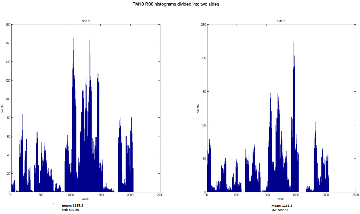
I wanted to test the chips in TM01, TM10 and TM11 modes (each TM in all ranges - from 3 to 12 pC). I have gathered many data in each mode (eg. 65536) and created histogram of the collected data. What surprised me is that the standard deviation is relatively high. Below is an example of the TM10 test. Please look closely at the R01 (R00 is similar) histogram. Besides values around the mean value there are some peaks from 0 to 2000. RANGE[10] (12 pC) looks completely different and the standard deviation is acceptable.

Basically what I expected from the measurements was gaussian shape of the histograms. It is not only not gaussian, but there are values that are far from the real one (but average value from many data is correct). Without averaging the measurement error is high.

Has anyone had similar problem? I can provide detailed information about DDC316 configuration if needed.

  • Janusz,

    Thanks for contacting us. I am applications support for the DDC316. Please let me look into this and I will let you know what other information I need from you.

    Regards,

    -Adam Sidelsky
  • Janusz,

    Since we don't offer a DDC316 EVM, I assume you are using your own board? Are the plots including both A-side and B-side data? We know there is an offset between the two sides as mentioned in the datasheet.

    Please let me know your integration time, CLK speed, DCLK speed, and 16-bit configuration settings.

    Regards,

    -Adam
  • Thank you for your reply, it's good to hear from you. Yes, we've manufactured our own board. Below are asked details. Please let me know if you'd like to obtain more information:

    CLK = 39 MHz

    DCLK = 39 MHz

    CONV = 5 kHz (thus tINTA/tINTB = 100 us)

    configuration settings = 1 000 01 0 1 10 0 1 0000 (of course range and TM is programmable).

    In other words:

    MODE = 0

    RES = 00

    RANGE = programmable

    nHI_SPEED = 1

    TM = programmable

    BUFDIS = 1

    Below you can see what happens if we separate data to A and B side. Both integrators behave exactly the same.

  • Thanks for the information. Have you tried adjusting the readout timing relative to the CONV window to see if it changes the output? Also you are not using the internal buffer, could you try using it?
  • What do you mean by adjusting the readout timing? If you mean adding a delay between nDVALID going low and start of DCLK then it's no problem, we can try that.

    It's harder with the internal buffer. We've designed the external buffer exactly as it is in the datasheet (Figure 15). It looks OK for us (maybe we can provide some oscilloscope screenshots, I'll check). If adjusting the readout timing won't work, then we will try to change to the internal buffer, but this will be a major modification and will take some time.
  • Janusz,

    Yes this is what I mean by adjusting the timing. For the buffer I don't think you need to make the big modification, just check with a scope that this signal is consistent. 

    Regards,

    -Adam

  • OK, we'll do the test but not until next week due to Easter. I'll let you know what's what on next week's Wensday/Thursday.

    Best Regards

  • Hello Adam,

    we've delayed data read as you suggested although there is another problem.
    In each conversion cycle we write the configuration register. We start writing after receiving the last bit of the conversion data. After we've delayed the data read DDC316 does not return configuration register data. We expect second nDVALID signal before CONV toggles. Instead, the nDVALID goes low right after the start of the next CONV cycle. What is wrong?

    In the DDC316 reference there is: "Writing and reading must be done before or after CONV toggles." - maybe we don't understand this sentence. It would be nice to see serial interface timing (Figure 1.) and configuration register read/write timing (Figure 2.) on one diagram.
  • Janusz,

    We do not show these two waveforms together because the two operations usually do not occur at the same time. Usually the device is configured and then some time later the device is used for integration. Are you re-configuring the device every CONV cycle before taking data? Or just configuring once and then taking data repeatedly afterwards?

    Some description of your config/integration cycle would be helpful as well as some scope shots or timing diagrams.

    Regards,

    -Adam
  • Adam,

    we reconfigure DDC316 in each CONV cycle but after the data read (this way we were configuring DDC316 for the next cycle) and before CONV toggles. This worked before delaying data. We thought that we were satisfying the condition "before CONV toggles".

    Reconfiguration in each cycle is due to the way we use our board - we program DDC316 on the fly with jumpers for easier switching between normal mode and test modes. I will try to  supply our config/integration cycle diagram/scope later but as I said before, we reconfigure in each cycle after the data read but before CONV toggles.

  • Adam,

    we reconfigure DDC316 in each CONV cycle but after the data read (this way we were configuring DDC316 for the next cycle) and before CONV toggles. This worked before delaying data. We thought that we were satisfying the condition "before CONV toggles".

    Reconfiguration in each cycle is due to the way we use our board - we program DDC316 on the fly with jumpers for easier switching between normal mode and test modes. I will try to supply our config/integration cycle diagram/scope later but as I said before, we reconfigure in each cycle after the data read but before CONV toggles.
  • Sorry for dobule (even triple) post. Here is a drawing of one conversion cycle. I don't have a scope nearby so this is the only thing I can do for now ;) Every conv cycle looks like this. At least it looked because now the second nDVALID goes low after CONV toggles.

  • Janusz,

    I think you are putting the device in a weird state by doing this. When you run DCLK after DVALID has gone high in a CONV cycle, you are telling the device that you want data to be output on the DOUT pin. You are then feeding it new configuration settings in the same CONV cycle. Usually we configure the device in one CONV cycle and then wait a few CONV cycles before beginning data readout. Do you have the option for this? I would try at least configuring in one CONV cycle and waiting until the next to readout data. Doing the operation in one cycle might be possible but it's not something that we do and I cannot comment on how well it will work. The same configuration settings should also be used for both Side-A and Side-B data, or in other words, for both one high and one low CONV pulse. It looks to me like the DVALID issue you are seeing is because the device is expecting to give you the B-data next but you are reconfiguring it before it has the chance to. Usually in a cycle that we are reading out data, we will lead with the DCLK toggling and the device will give us data. In a cycle we are changing the configuration, we lead with the DIN_CFG data and only clock DCLK at the end if readback is required.

    If you want we can have a call to discuss.

    Regards,

    -Adam
  • Adam,

    thank you for the explanation. I'll let our constructor know about this. It is not a problem to change the program to realize what you've described. After the modification and tests I will post an update.

    Best regards,
    Janusz