This thread has been locked.

If you have a related question, please click the "Ask a related question" button in the top right corner. The newly created question will be automatically linked to this question.

DRV8303 control register1 resets automatically after configuring it successfully.

Other Parts Discussed in Thread: DRV8303, DRV8301

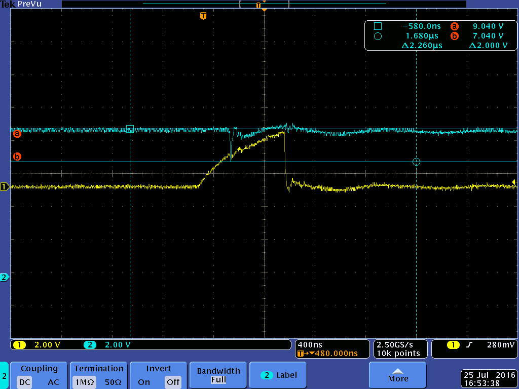
We are trying to configure the Control register 1 of DRV8303 with the hex value 0x128A. We are operating on Current limit mode.

We have observed that for once it configures the CR1 correctly and we have verified it by reading back the value from the DRV8303 IC.

But once we read-back  its successful configuration(which is read only once) , if we try to continuously read-back the configuration from the DRV8303 we find its configuration resets or sets to a hex value 0x1400.

We have read the datasheet and verified the voltages to be correct as follows:

AVDD : 6.73V

DVDD : 3.4V

GVDD : 10.96

En_GATE : High

PVDD : 24V

Can we get some help on what could be the reason for the problem we are facing?

Moreover

  • Hi Jeeva,

    Your description is indicating the SPI has been reset.

    There are a few items to check.

    Are you writing to Control Register 2 also? Is it being reset?

    Is there some method that you can use to capture the reset event? An example would be configuring an underused current shunt amplifier such that it reads approximately 0V when in operating mode. Then place the amplifier in calibration mode during operation. If the device is reset, the amplifier will drop out of calibration mode providing a trigger for the scope.

    According to section 7.3.3.3 of the datasheet, a PVDD_UV event will cause the SPI registers to be reset. Please check for an undervoltage event.

    What is the voltage on VDD_SPI? Is it possible that it is drooping, and causing the SPI to reset?

    Are you monitoring the nFAULT signal? Does it assert?

    If you are still having troubles, feel free to provide scope captures and the schematic.
  • We a trying to drive a stepper motor using DRV8303. We are interfacing and configuring the DRV IC using micro controller. We have configured DRV8303 in 3 PWM mode. We checked the MCU output for PWM and it shows correct values. We also checked the DRV output for PWM which was correct and it was generating complementary output which was required as per the configuration. But this condition was satisfied till we have not mounted any MOSFETs on our board. As soon as we mounted the MOSFETs on our board we saw that the DRV's PWM output disappeared from the lower MOSFET and the high MOSFET was showing a very low voltage square pulses which was not matching with our PWM input to the DRV.

  • Hi Jeeva,

    Is this the same board as the previous post? If so, would you mind if I merge the threads?

    Have you looked at the PVDD voltage?
  • Hi Rick,

    Yes its the same board as the previous one. You can merge it to the previous Thread.

    We measured the PVDD and its values is 24V as expected and VDD_SPI is 3.3V. We made one more observation on our previous question, if we try to read the control register1 multiple time i.e more than 2 times in a continuous loop, then the value of CR1 changes. We tried to write and read the CR1 continuously in a while(1) loop and the read back was not correct it was showing us a value 0x1400 instead of 0x128A. We have tried to run something similar with DRV8301 evaluation board and we could continuously read-back a correct value in a infinite loop as well.

    Thanks

  • Hello Rick,

    Thank you for swooping in to help us out. And sorry about the mixup in posts.

     As a response to the points raised by you,

    1) We have checked for PVDD undervoltage. We don't notice any PVDD under voltage on board.

    2) We don't see VDD_SPI drop.

    3) Fault is asserted. And we see repetitive toggle on both nFault and nOctw. Their assertions seem to be happening alternately.

    Also we did the following:

    1) Checked for Gate drive outputs in the 6PWM mode and found that the readback value did not change over repititive readbacks. So we proceeded to test for gate drive outputs for that configuration and noticed the following:

    a. At the Gate of the High side MOSFET, we don’t see the expected output corresponding to the PWM inputs provided. The pulses of output amplitude, at around 3V is seen, without any match in the PWM frequency or duty cycle.

    b. We notice no gate drive output at the Low-side MOSFET. It is continuously LOW.

    c. We see that nFault is toggling with only short periods HIGH. nOctw is continuously HIGH.

    2) Checked for PWM without SPI configuration, with default settings.

    a. We provide 6 PWM inputs to the DRV. (Considering the default configuration)

    b. We notice Improper pulse outputs ( not expected PWMs, improper frequency, improper duty cycles) the amplitude of the pulses on the gate of the Top side MOSFET was around 10 V and the bottom side gate, pulses were of around 5 V amplitude.

    c. We see that the nFault is toggling, it stays LOW for most of the time. nOCTW is continuously HiGH.

    What could be the problem we see? Please provide your opinions.


    Regards.

  • Hi Jeeva,

    I think we should focus on the faults first. This should not be occurring. Please look at table 4. From your description, the most likely faults are PVDD, DVDD, or GVDD undervoltage.

    Please zoom in on the scope and capture these signals prior to the nFAULT pin asserting.

    Once the fault is corrected, the next step is to work on the registers.

    Is the power pad connected to GND? If not, it must be.
    If you think the schematic or layout could be an issue, can you send the schematics and layout?
  • Hi Rick,

    Yes, the power pad is connected to ground.

    Please find the relevant schematics below:

    Below is the capture of nFault spikes (Yellow waveform) and the Gate drive outputs PWM_AL (Blue waveform) . THe PWM inputs are 32kHz square waves. DRV is configured in 3 PWM mode, current limit mode.

    We have zoomed in on the captures of nFault w.r.t GVDD. PVDD and DVDD.

    1) PVDD (Yellow waveform, after AC coupling)  w.r.t nFault (Blue waveform)

    The spikes seen are of a few hundred millivolts, which we believe should not be the cause of an undervoltage lockout.

    2) DVDD (Blue) w.r.t nFault (Yellow)

    There is a drop of around 1 V.

    3) GVDD w.r.t nFault

    Please provide your opinions.

    Regards.

  • Hi Jeeva,

    Thank you for the scope captures. If I am reading them correctly, nFAULT is low most of the time. That is the item where you should be focused.

    Once this is corrected, the spikes on nFAULT should not occur because nFAULT will be high.

    There is one item of concern in the schematic. The numbering of pins 19 and 20 are out of order. Please check that the schematic and layout are correct in this area.

    If it is correct, please disconnect the motor and slowly proceed through the procedure to turn on each pair of FETs.
    Once the SPI registers are configured, monitor nFAULT.
    When does nFAULT assert (go low)?
    1) Set EN_GATE high
    2) Set INL_A high with INH_A low
    3) Set INL_A low and INH_A high
    4) Set INH_A low
    5) Repeat steps 2 through 4 with INx_B and INx_C
  • Hi Rick,

    Regarding the pin numbering, we have checked the routing and it looks fine, only the pins are swapped (in the schematic).

    We tried the sequence you mentioned. We saw that at step (2) the nFault was reported (for all the branches A, B and C). nFault was HIGH for the rest of the cases.

    But will this test sequence take into account the effect of the Bootstrap capacitor on the turn-on of the top mosfet?

    When we toggle the on-times (HIGH) on mosfets AL and AH continuously, we see that the fault is reported most of the time (as shown in the screen captures). Doesn't that mean that if the bootstrap capacitor remains charged, only then the top mosfet can turn on? And so the fault continues... So, we think any MOSFET turning on, is causing a fault. But when we try to readback the status registers, we see that they are all zeros on SR1 (status registers) and no GVDD UV fault on SR2, representing no faults.

    Your opinions have been helpful so far, please let us know what you think.

    Regards.
  • Hi Jeeva,

    Thank you for the information.

    The test sequence does take into account the bootstrap cap, but there is a more fundamental problem. If turning on the low side FET asserts nFAULT, the bootstrap cap will not be charged.

    Step 1 is an indication the regulators have powered up properly.
    Step 2 should then pull the output low and full charge the bootstrap cap. If nFAULT asserts on step 2, something is incorrect with the phase connections.


    After the device is powered, add a 5k to 24V/15k to GND resistor divider from 24V to GND. Connect the midpoint to the SH_A output. SH_A should measure approximately 18V before step 2. Does it?

    If not, what voltage is measured? Where does this voltage come from?

    If 18V is measured, perform step 1 to enable the regulators.
    Then perform step 2 while monitoring the GL_A, SH_A, and SL_A pins. With INA_L high and INA_H low, GL_A should be approximately 11V. SH_A and SL_A should be approximately 0V.

    Can you provide scope captures of the outputs when IN_A is set high?
  • Hi Rick,

    We have performed the tests as suggested by you and have several snapshots for the same.

    We have connected the resistor divider as suggested.

    Test Case0: We turned on our board with the resistor divider whose midpoint is connected to SH_A, before enabling the DRV IC using EN_GATE.

    EN_GATE = 0

    Measurement : SH_A with respect to GND is 6V

    Query : We did not understand why the SH_A is 6V even before enabling the EN_GATE


    Test Case1 : We turned on our board with the resistor divider whose midpoint is connected to SH_A, enabled the DRV using EN_GATE = 1 and configured it.

    Measurement : SH_A with respect to GND is 18V


    Test Case2 : We turned on our board with the resistor divider whose midpoint is connected to SH_A, enabled the DRV using EN_GATE = 1 and configured it and we set INL_A = 1 and INH_A = 0

    Measurement :

    (Refer to the images below)

    GL_A : 10.4V rising pulses with ns on period

    SL_A : Spikes falling from 0 to 600mV

    Sh_A : Spikes falling from 0 to 6V

    NOTE : You have suggested that the results for SH_A would be ~0V when the lower mosfet on but we see that before the Mosfet is on the SH_A is 0. When we see gate pulse of the lower mosfet the SH_A is falling from 0 to 6V as shown in the pictures below.

    Query: When mosfet is off are we expecting SH_A with respect to GND to be 18V or 0V since the resistor divider is connected?

    In the images below:

    Channel 1(Yellow) is GL_A

    Channel 2(Blue) is SL_A

    Channel 3(Pink) is SH_A

    Regards,

    Jeeva J

  • Hi Jeeva,

    I will have to look into this on my end. This may take a couple of days to research.

    We still need to determine the cause of the nFAULT before proceeding to driving the motor.
  • Hi Jeeva,

    Test Case0: We turned on our board with the resistor divider whose midpoint is connected to SH_A, before enabling the DRV IC using EN_GATE.

    EN_GATE = 0

    Measurement : SH_A with respect to GND is 6V

    Query : We did not understand why the SH_A is 6V even before enabling the EN_GATE

    I see the same thing on the bench here. There is a sneak path of approximately 3k between the SH_A and ground when the device is powered but EN_GATE is low. I had overlooked this path when asking you to measure 18V.

    Test Case1 : We turned on our board with the resistor divider whose midpoint is connected to SH_A, enabled the DRV using EN_GATE = 1 and configured it.

    Measurement : SH_A with respect to GND is 18V

    I see the same 18V here.

    Test Case2 : We turned on our board with the resistor divider whose midpoint is connected to SH_A, enabled the DRV using EN_GATE = 1 and configured it and we set INL_A = 1 and INH_A = 0

    This is different. The SH_A pin is a solid 0V with nFAULT 3.3V (no spikes).

    Is it possible to get your layout so we can look for differences that could cause this?
  • Hi Rick,

    Thanks for the information. Can we have your mail ID so that we can share the layout.

    Regards,
    Jeeva J
  • Hi Jeeva,

    I will send you instructions soon.
  • Hi Rick,

    Thanks for your help in looking into our design layout.

    Here are few observations regarding bootstrap capacitor.

    Test condition: All 6 MOSFETs are removed from our board. DRV is configured in Current Report Only mode, so no action is taken on OC faults.

    Scenario 1) We disabled gate pulses on a Half bridge (by removing gate resistors of MOSFET) and verified two sides of the Bootstrap cap on that Half bridge.

    At the driver side of the bootstrap cap, we noticed a constant DC voltage of around 34V with respect to GND. At the MOSFET side of the Bootrap cap (SH_A) we see 24V DC with respect to GND.

    Scenario 2) We enabled the gate pulses on the MOSFETS of the same Half bridge. (Enabled both High and Low side MOSFETs)

    And on the Driver side of the Bootstrap we see the following waveform with respect to GND:

    On the MOSFET side of the bootstrap capacitor we see the following waveform with respect to GND:

    This is what we noticed without MOSFETs.

    We tried monitoring the Bootstrap cap on our DRV8301 Eval Board where we are able to rotate our stepper motor successfully at lower speeds,

    1) We found that upon Isolating the MOSFET gate from the driver, we see similar DC levels at the bootstrap cap.

    2) Without isolating the MOSFET gate from DRV8301 we noticed PWMs (34V HIGH, 10V LOW)  similar in period and voltage level to that of Gate Drive pulses.

    And on the MOSFET side of the Bootstrap Capacitor  we saw the same waveform with a 10V shift downwards (24V HIGH, 0V LOW). (Similar to above waveforms.)

    Can you suggest what can cause problem in our board having DRV8303? Do you have any tests you would like us to carry out?

    This issue is getting very critical, expecting your continued support.

    Regards,

    Jeeva


  • Hi Jeeva,

    Was the fault removed after removing the FETs?

    If it was, please install each FET one at a time. Then look for a difference in behavior.

    I looked through the schematic again, and noticed the AGND and PGND are not directly connected. This could cause a the voltage on the digital side to collapse. As another experiment, please try connecting pin 24 to pin 49. A good location is the bottom plate of C18 to the thermal pad.

    Have you tried a second board? Does it exhibit the same behavior?
  • Hi Rick,

    Thank you so much for your help.

    As you suggested we have connected AGND and PGND directly and we see the expected output. we have tested on other boards connecting the grounds directly. all boards are working as expected. Sorry for the late reply.

    Regards,

    Jeeva J

  • Hi Jeeva,

    You are welcome. We are glad to hear your boards are working.