This thread has been locked.

If you have a related question, please click the "Ask a related question" button in the top right corner. The newly created question will be automatically linked to this question.

DRV8303: DRV8303 Flow Through Drive of High and Low Side FETs

Part Number: DRV8303
Other Parts Discussed in Thread: BOOSTXL-DRV8301, CSD18540Q5B, DRV8301, CSD19532Q5B

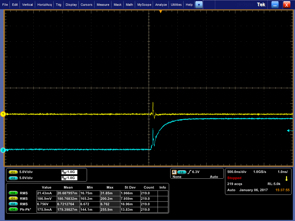
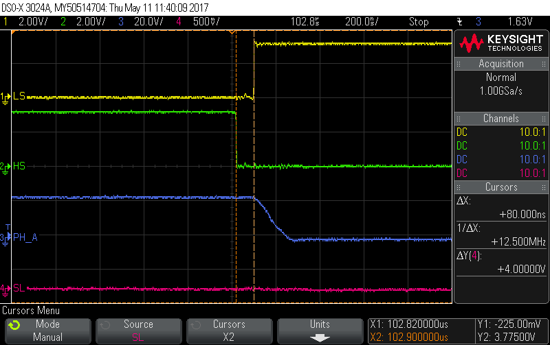
We are using theTMS320F28069MPZT and the DRV8303 and have a problem with the GLx (lower gate output drive) spiking up when there is a transition on the GHx signal (high side gate output) the result is high currents (3V/0.025 ohms = 120A!) flowing through. The Rsense in this circuit is 0.025ohms. Increasing the dead time has no effect on the GLx output drive spiking high. We had the boards x-rayed to confirm that the exposed pad of the DRV8303 was properly connected to the ground plane.


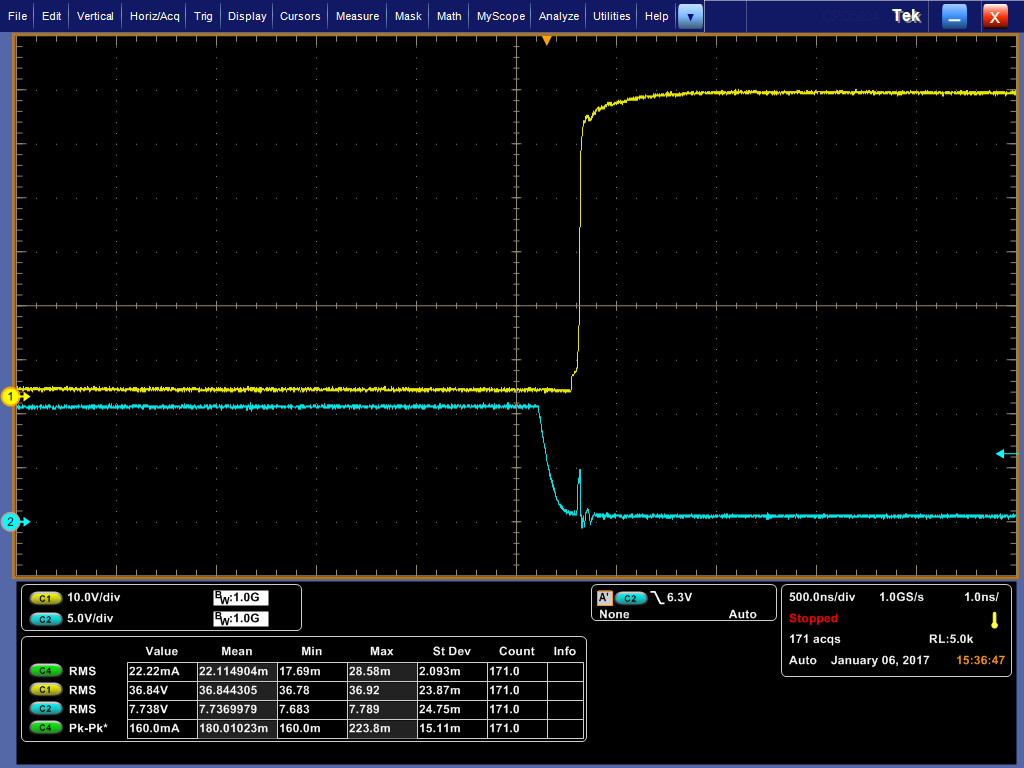
We then set up the BOOSTXL-DRV8301 board and it behaved similarly; high current spikes on the edges of the high side gate drive.  We are very careful with our scope grounds and confirmed that what we are measuring is truly present.


For the following images, the FOC software was set in the RS Recalibration mode for Motor Identification. The motor isn’t spinning. However when the motor is spinning, these spike are still present. 

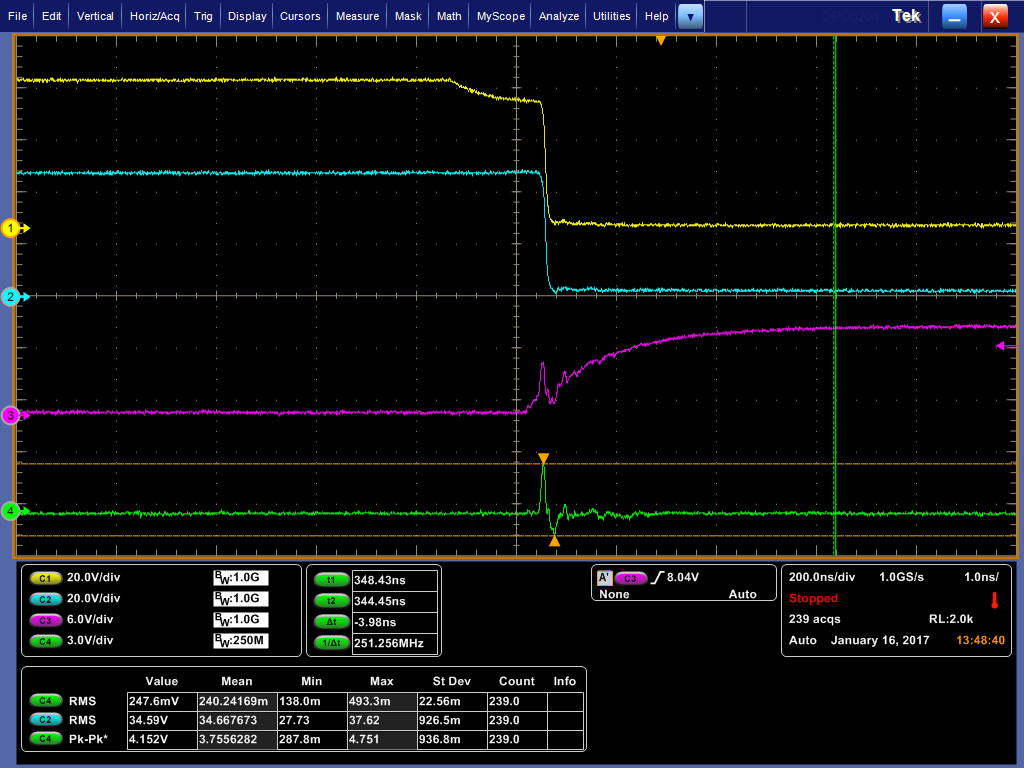
DRV8303 GH Falling and GL Rising

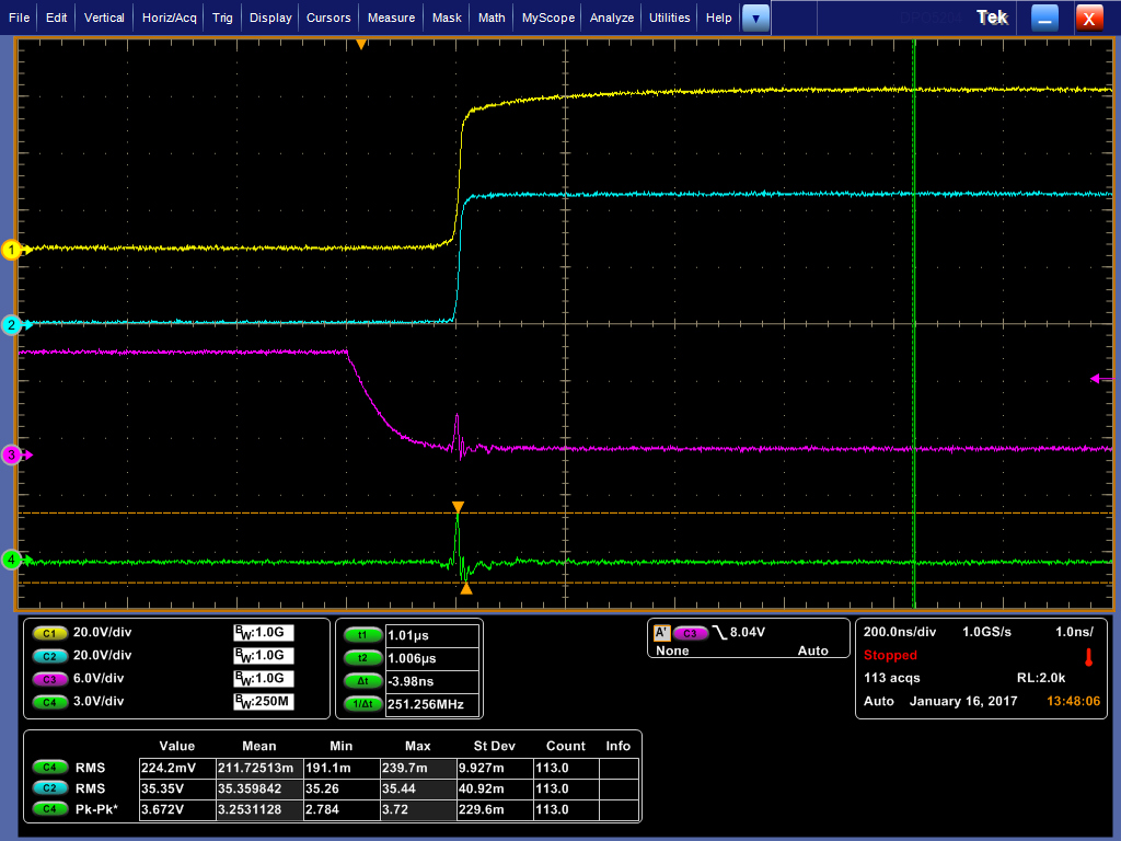
DRV8303 GH Rising and GL Falling

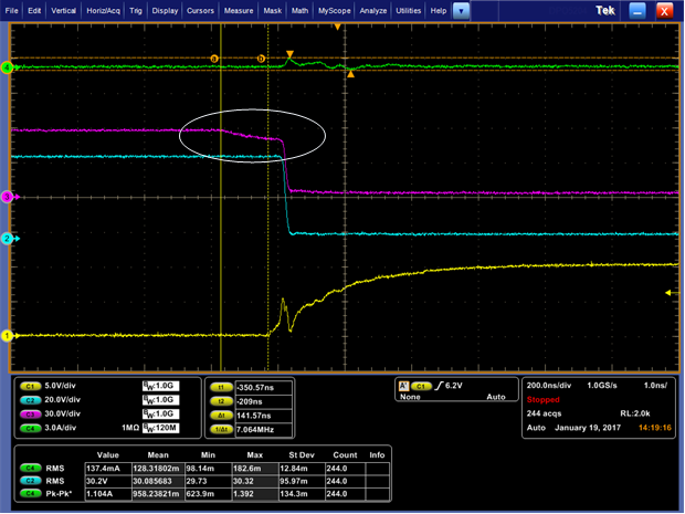
DRV8303 GL Falling and Voltage on RSense

DRV8303 GL Rising and Voltage on RSense

  • Hi Steve,

    We will investigate, but this may take a few days.

    What are the register settings used?
    What FETs are being used on your board?
  • FETS: TI CSD18540Q5B
    Series Gate Resistance: 10 ohms
    PVDD: 48V

    Control 1: 0x0542
    Control 2: 0x0000

    Gate drive peak current: 0.25 A
    PWM mode: 6 Inputs
    OCP mode: current limit
    OC adjustment: Vds 0.730 V
    OC/TW mode: both
    Shunt gain 10V/V
    DC cal mode Ch1: load
    DC cal mode Ch2: load
    OC Off Time mode: cycle-by-cycle

  • Hi Steve,

    Thank you for the additional information.

    The high dV/dt transitions from the GHx signal look to be the cause of the transient observed in your initial post. I would recommend two possible solutions to try and mitigate this problem:

    1.) If possible in your solution, slow down the switching speed of the GHx MOSFETs by increasing the gate resistor values. This will limit the gate current to a smaller value and slow the slew rate of the high-side MOSFETs.

    2.) If slower slew rates are not possible, adding external pulldown resistors on the gates of the MOSFETs will help stop the low-side gate voltage from rising up during the high dV/dt transition.
  • Can you explain how the falling edge high dV/dt transitions of the GHx MOSFET causes a positive pulse on the output from the DRV8303?

    We did increase the gate resistors to 20 ohms, from 10; but it had no effect. Our concern with going higher will be heat lost in the TI MOSFET. At 45KHz PWM, what is the maximum resistance the TI MOSET can safely handle?

    What is a recommended pull down for the GLx outputs of the DRV8303?

  • TI,

    Do you have an update as to why the DRV8303 (and DRV8301) have this undesired behavior of shoot-though, caused by a narrow pulse out of the low-side gate drive output?

  • Hi Steve,

    I apologize for the delay in response and appreciate your patience.


    1.) Have you tried increasing the DTC resistor value in your design? I saw that you said you've tried increasing deadtime, is this resistor value what you've adjusted?

    2.) Have you tried adding 10k Ohm Pull down resistors on the low-side Gates?

    3.) Does increasing the high-side gate resistors to a value around 40 - 50 Ohms decrease the voltage spike measured?

  • Phil,

    1) The DTC resistor (pin 3) is the value that I increased. As it was increased, the flow through spike moved with the increased time.

    2) I tried pull down resistors down to 250 ohms, with no effect.

    3) I increased the gate drive up to 20 ohms, with no effect. I'll try at 50, but because of the high PWM frequency, this is not likely to be an acceptable solution if it works.

    We use a circuit that is nearly identical (same driver, same FETs) to the one used in your 1-kW/36-V Power Stage for Brushless Motor in Battery Powered Garden and Power Tools (TIDU708) app note. Figures 26 & 27 show this flow through spike. I want to know the fundamental reason (what electrically is happening to the driver) for this behavior.

    Increasing the gate drive peak current from 0.25A to either 0.7A or 1.7A causes the flow-through current in increase.

  • Hi Steve,

    Thank you for the information.

    Have you been able to make these measurements with a differential probe? I'm curious if the Voltage we're looking at is real or if it's possibly an artifact.

    To your point, the negative slew on the GHx pin should not cause the positive transient measured on the GLx pin. Also, the Voltage measured on the SLx pin (RSENSE) violates our absolute maximum rating, so if the 3V measured on SLx were real it would most likely damage our part.

    I'm headed to our lab now to recreate this measurement with a differential probe and normal 10:1 probe, I will report my findings as soon as I have them.
  • Here is a scope (2GHz bandwidth) image using a differential probed (3.5GHz bandwidth) across the R-Sense Resistor.

  • Hi Steve,

    Thank you for the scope capture. I have a couple other requests:

    1.) Could you get a scope capture of Phase A / GHA / GLA / RSENSE? The 500 ns timescale you used previously is fine.
    2.) What VM voltage are you performing this testing at?
    3.) Is this test done with a motor connected?
  • 1) The scope captures above were for Phase B. The images are the same for Phase A. Should there be a difference between Phase A & B?

    2) 48V is being used. I noticed that reducing the voltage to 24V did reduce the GL_X output pulse of the DRV8303.

    3) A motor is connected.

  • Hi Steve,

    I apologize, I meant the SHx Voltage. If possible, I would like to see the SHx Voltage with the GHx and GLx voltages. It can be on any phase.
  • 1) The scope images above we for Phase B. They are the same on all the phases. Should phase A have different behavior?

    2) We are using 48V for the drive system. When we reduced this voltage to 24V, the low side gate drive pulse from the 8303 was reduced.

    3) Yes, a motor is connected.

  • Trace 1: GH_B
    Trace 2: SH_B
    Trace 3: GL_B
    Trace 4: Rsense (7.1mohm)

    Motor connected, the FOC software was set in the RS Recalibration mode for Motor Identification. The motor isn’t spinning. However when the motor is spinning, these spike are still present.

  • Hi Steve,

    I spoke with our designer about the way we implement our internal pull-down resistor on the low-side gate during a high-side gate switching event.

    On this device, the internal pull-down resistor is not strong enough to keep the GLx pin held down with how quickly the GHx pin is slewing. The CSD18540Q5B MOSFETs have a low QGD, which allows them to slew very quickly with minimal gate current.

    In the case of your 48V system, the transient coupled into the GLx line is enough to slightly turn on the low-side FET, causing a brief period of shoot through measured by the large transient on the RSENSE line.

    I would recommend significantly reducing the slew rate on the GHx pins. Currently, it looks like you're slewing almost 36V in 10 ns. I would recommend increasing the series gate resistor value until a slew rate of approximately 40 - 50 ns is achieved. This should significantly lower the coupled transient and stop the shoot through measured on RSENSE.

    At your desired switching frequency of 45 kHz, a rise time of 50 ns should be negligible in comparison to the 22 us period of your PWM signal.
  • Phil,

    In addition to increasing the slop of the GHx pins (increased gate resistor), the dead time would also need to be increased. Correct?

    The dead time can be increased using the DTC resistor of the DRV8303 and it can be changed using the parameter in the InstaSpin-FOC motion software. Does the InstaSpin-FOC motion software need to control the dead time? Does it matter to the InstaSpin-FOC motion software how the dead time is added?

  • Hi Steve,

    You may need to make some deadtime adjustments, but the DRV8303 will measure the voltage on the GHx and GLx pins for when the Vgs voltage is below a specific OFF threshold. Once below this threshold the deadtime timer is started. So, you may need to make some deadtime adjustment but shouldn't need to make any large increases.

    I would recommend making the change in the software to make the tuning process easier.
  • Can you model the DRV8303 with the CSD18540 FETS?

    Increasing the high side gate resistance increases the slope in the area circled below, but does not affect the falling edge, which ‘waits’ for the low side to start conducting before it falls and the gate resistance has no effect on this slew rate.

    Secondly with a higher gate resistance, the FOC software in the RS Recalibration mode for Motor Identification will drive the FETs in such a way to burn out a set of top & bottom FETs. This, in spite of the fact that the DRV8303 is not supposed allow this. How can the InstaSpin software, with the DRV8303, turn on and short out a top & bottom FET?

  • Steve... all your measurements and findings mirror the exact issue I have been having with the DRV8303. I have even gone to the extent of reducing GH and GL trace coupling trying to solve this. Increasing the slew rate helps on high side turn on, however subsequent excessive DTC does not help on turn off.

    I am disappointed this thread has stopped before a solution was found.
  • I am using 2x CSD18540Q MOSFETs. Slowing the high side slew rate from 10ns out to 50ns with a 100R series gate resistor made a significant improvement in reducing the low side ringing issue. The shoot through on high side switch off did however become a fault inducing issue. I have tried several combinations with both high and low gate currents. The unfortunate issue is that there is a need for a slow charge to prevent the low side gate ripple from high dV/dt, yet need a fast discharge to prevent shoot through. It appears the DTC control does not work as intended. I haven't otherwise been able to determine (based on the datasheet contents) the mechanism for investigating the DTC trigger condition.

    2.2k resistor pull downs have no noticeable impact on either high or low side gates.
    A 4.7R series bootstrap resistor wasn't found useful in solving this issue.

    Using a 100R series resistor on the high side gate seems a stable approach for overcoming the low side gate ripple. The low side just can't hold itself off, even on the highest gate current setting or with resistor pull downs. For turn off, high gate current helps, but the subsequent shoot through gets worse. Having the DTC at maximum or shorting to 0R dynamically has no impact at all on the shoot through condition. Fitting a schottky diode in parallel with the high side gate resistor to discharge the gate quicker is a noticeable improvement, but still does not solve the shoot through.

    Currently I can only conclude that the DTC cannot be used to prevent the observed shoot through. Perhaps with detailed information on the DTC mechanism this could be checked further. Otherwise, it appears the design needs to use a 6-PWM control signal with digital deadtime adjustment. Unfortunate, as the software for the space vector modulation output was already completed and validated.

    Any feedback on the DTC would be appreciated!
  • I would really appreciate some feedback.  Having great difficulty getting this DRV8303 gate driver to function as intended.  It keeps causing shoot through and then faulting.  Spent over 2 days working on this issue and now nervous for possible design set back.

    Probe for SL used spring clip for ground across sense resistor.

  • I have moved to testing different MOSFETs with higher gate turn on thresholds.  CSD19532Q5B.  I don't want to use these, as they have higher Rds(on).

    It doesn't matter how much dead time I introduce.  Below is an example where with the use of deadband in the control signal inputs, 1.5us.still doesn't solve the issue.

    The motors commutation glitches with all the resulting faults.

  • It is/was unfortunate that TI discontinued their responses. It was also a little disconcerting that this behavior was observed in a few of TI’s reference designs (their own app notes showed it), yet they didn’t think it was important enough to solve or comment on. I was hoping that they could use their spice model (which I’m sure they have for the chip & their transistors) to simulate this case and provide some guidance. The glitches we were observing didn’t affect the operation of the driver system, but produced unwanted EMI. We observed also that dead time has no affect.
    I did simulate (LTSPICE) the output topology (high & low side fets, with floating high side gate drive) and saw similar flow through current. I was only using the fet models in their library, so I couldn’t simulate the TI transistors.
    What appears to be the cause, is that the floating high side drive goes to zero (gate to source), but the voltage on the source of the high side fet is still high & won’t get discharged until the low side fet is turned on (which is why dead time doesn’t help). As soon as the low side drive voltage is high enough to turn on the low side fet, the charge held in the high side fet is discharged, causing the spike.
    We used various FETs from the LTSPICE library and did find one (Infineon) that ‘worked’, in both the spice model and on a real board. It had lower capacitance and slower rise & fall time and (unfortunately) higher on resistance. I think it is the lower capacitance and slower rise/fall time that reduced/eliminated the spike. We accepted the added heat penalty for lower emi.
  • This is classic "Miller Effect".  The low-side fets need a diode across their resistors too.  That way you can use larger gate resistors to slow the turn-on of the fets without compromising the ability of the gate driver to clamp the gate low as the other fet turns on.  This is prevalent throughout the industry, and the TI people should have been attuned to it...  Good luck!

    Regards,

    Dave

  • Thanks Steve.  Really good to get your validation and outcome on the problem.  Appreciate the reply!   Slower rise times have helped a little, although I'm reluctant to accept the heat in this application as the design doesn't accommodate for it.  I can't see controlling the the high dV/dt on the high side source when it's pulled low is practical, but I can see your solution of using a FET with lower capacitance would help.

    I have had a lot of trouble with the associated shoot through current causing OC faults.  I can see it across the sense resistor.  Even with the OC_ADJ_SET to maximum I have been getting some intermittent overcurrent faults.  Had to disable the feature - which is not ideal.  EMI from this might be problematic.

    Dave, I like your idea.  I'm going to try some schottky diodes.  Perhaps also consider if a snubber could be used.

  • Hi Eclipze,

    As I stated to Steve Riley on January 18th of this year, this issue can be solved by correctly sizing gate resistors for the MOSFETs selected in your application. The spikes on the gate signals are artifacts of slewing the MOSFETs to quickly, which as I said, can be solved by selecting different gate resistors and slowing down the gate transitions. This is independent of the DTC resistor value selected.

    The DRV8301/2/3 devices are all our first-generation BLDC Gate-Drivers that only offer three different Source / Sink current settings. Our new generation devices have much more room for adjustment on the Source / Sink gate currents that the device will supply as well as integrating a strong pull-down current of 2 A for a time interval when the opposing gate begins slewing in a 1/2 bridge configuration.  This is intended to prevent the type of behavior described in this thread.


    Our new generation 60V BLDC Gate driver that is comparable with the DRV8303 would be the DRV8323S. The datasheet for this device is available here:

    www.ti.com/.../DRV8323

    The integrated gate drive currents in the part are referred to as IDRIVE, we have an app note outlining proper shoot through prevention in inverter design and IDRIVE selection for our devices here:

    www.ti.com/.../slva714a.pdf

  • Thanks for your input Phil.  The DRV8323S looks of interest, however as a preview part it is not available for consideration.  The application note was however really good to read through.  I'II re-visit testing with slower gate turn on as you suggest, but this time with the use of diodes to help with stronger turn off.

  • Hi Phil,

    I have been watching for additional IDrive/TDrive parts as they are released.  Would it be possible to add this as a selection attribute on you web site?  I think they are potential game changers for many applications, especially since they can often eliminate *many* discrete resistors and diodes as well as provide SPI-based tuning and optimization.  They deserve all the hype you can give them!

    Regards,

    Dave

  • Hi Dave,

    Thank you for the feedback, this is definitely something we're looking into solving on our end as to how we can best position this technology on our website. Appreciate you following our releases as we incorporate this technology in more places.