This thread has been locked.

If you have a related question, please click the "Ask a related question" button in the top right corner. The newly created question will be automatically linked to this question.

DRV8825: Irregularities in output waveform

Part Number: DRV8825
Other Parts Discussed in Thread: DRV8880, DRV8886AT, DRV8886ATEVM

I am designing a custom controller board for controlling steppers on a telescope mount.  For my initial prototype (Rev A) I used two Pololu DRV8825 Stepper Motor Driver Carrier boards plugged into a custom board design.  This prototype drives two 1.5A NEMA 17 bipolar steppers and works very well. 

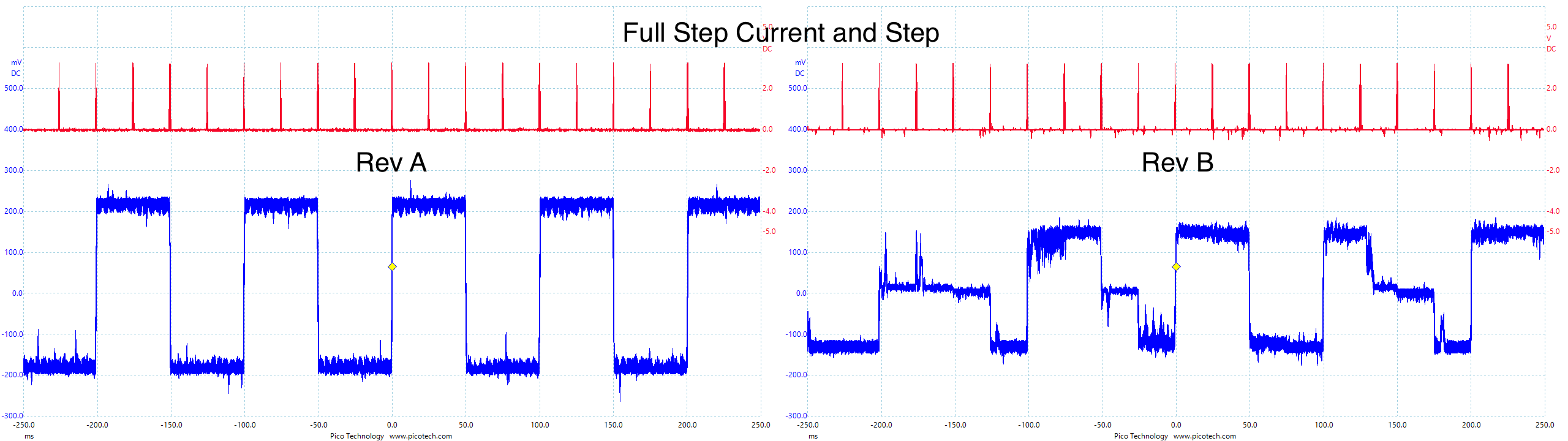
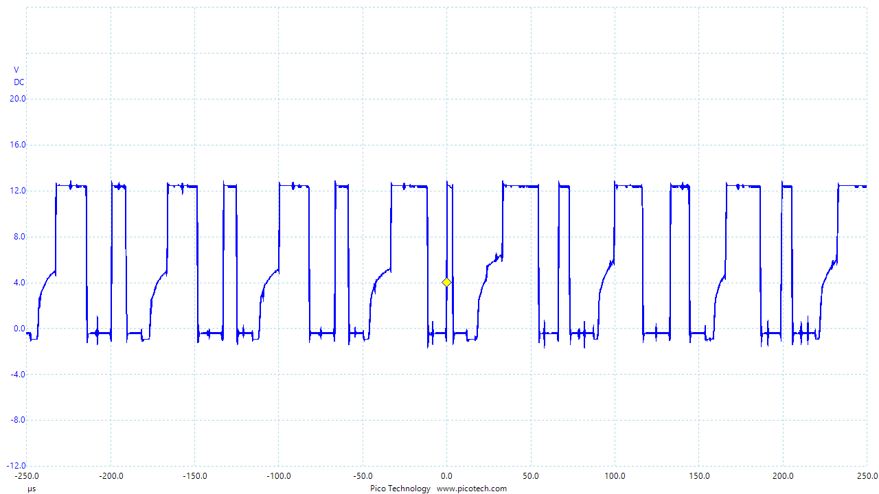
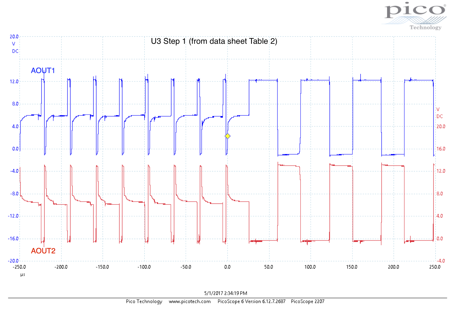
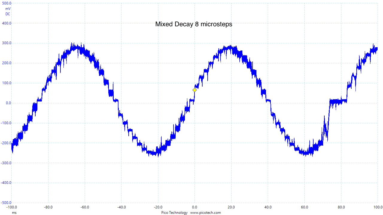
I designed a second board (Rev B) using three DRV8825 devices mounted directly on the board and I am experiencing erratic motion on all three motors and see some serious irregularities on the current waveform as shown below.  This trace was captured while in full step mode with a step rate of 40Hz. to a single NEMA 17 stepper.  The corresponding trace of the Rev A system looks good.

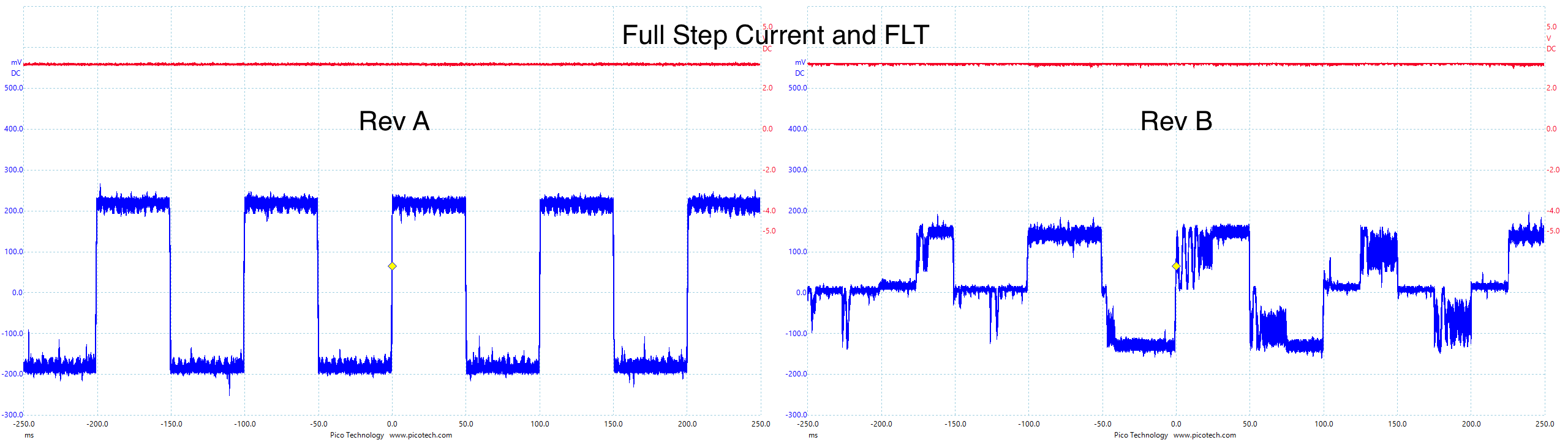
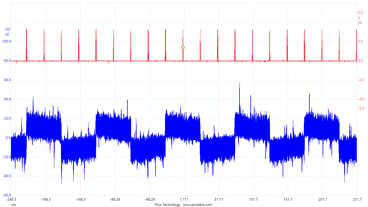
In looking further into the problem I also see serious irregularities in the PWM waveforms for both A and B outputs as shown below.  Again, the corresponding traces from the Rev A system look normal.

Details of the Rev B design are:

  • Three DRV8825 devices controlled by PIC18F46K20 microprocessor
  • Two NEMA 17 2.0A bipolar stepper motors, phase resistance 1.4 Ohms, phase inductance 3.0 mH
  • One Nema 11 670mA bipolar stepper motor
  • 12V power supply (same supply successfully used on Rev A board)
  • Decay is set to Fast Decay.
  • I used a stencil, solder paste, and a hot plate to do the reflow soldering of all components, monitoring the board temperature with an IR thermometer.
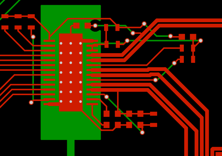
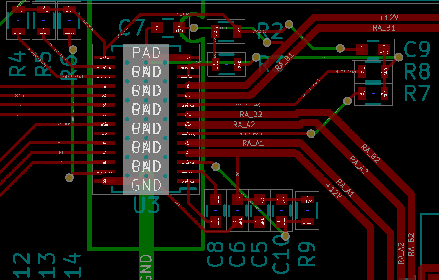
  • Schematic and layout shown below

The board as tested differs from this schematic as follows:

  1. Resistors R4 and R5 are tied to the board 3.3V net rather than the DRV8825's local 3.3V.  This was accomplished by cutting a trace and adding a wire.
  2. Resistors R7 and R8 are now 0.1 Ohm 0.5W.  The original resistors did not have an adequate power rating.
  3. A 100mF 35V electrolytic capacitor was added at the device.  The original design had a single bulk capacitor for the entire board.

I realize that much of the layout is not according to recommendations.  After reading most of the DRV8825-releated posts on this forum I realize that much needs to change here.  Previously I had not seen the EVM so I will use it as a model for the next rev.

I have tested all three DRV8825's on the board and they all show this behavior.  Has anyone seen anything like this in the past?  Is there anything in the information here that would point to a possible cause?  I will be redesigning the board in any case but I would like to have an idea of what caused this before I do that.  My only theory at this point is that my solder reflow method resulted in the devices getting too hot and being damaged.  It seems unlikely to me that all three devices would be damaged in the same exact way however.

  • I missed one of the mods in the list below the schematic: R2 is now 6.8K and R3 is now 2.0K. This gives me 1.5A max current.
  • Hello jcarter,

    Is your revB layout design very similar to your revA? If it is, then please isolate the 3rd device and see if you can successfully run the two motors from revA.
    If you are not successful I would go back to one device and even resolder a new device to see if is a layout issue or device soldering issue. Your Schematic snapshot looks okay.
    I see some problems in your layout and I think you are aware of them. Following the EVM layout is a good example to follow in your next revision.
  • Hello Luis,

    The Rev B design is similar to the Rev A except that on the Rev A the DRV8825 devices are on the Pololu carrier board rather than on my board as mentioned. For the testing thus far I only use one 2.0A motor. I can connect that motor to the Rev A board (adjusted for 1.5A max output), connect the power, and watch the motor work normally. I then take the same power supply and same motor, connect them to the Rev B board and see the erratic behavior I described. I repeated the Rev B test with each of the three devices on the board and I see the same result for each one.

    Have you had any reports of irregularities in the PWM waveform such as the ones I posted? Have there been reports of devices being damaged by overheating during the reflow process? If so what were some of the failure modes?

    Thanks for your help,

    John
  • Hello Luis,

    After looking more closely at your question about similarities in layout between my Rev A and Rev B, I think the answer is that they are not very similar with regards to the DRV8825 since the layout around that device was done by Pololu in Rev A and by me in Rev B.

    Thanks,

    John
  • Hello jcarter,

    Thank you for the clarification. I see the thermal PAD which connects to the GND is missing, it is recommended to have that thermal Pad to remove heat. One thing we can try is to lower the current so see if that is one of the problems.
    Could you please try running your motor around 300mA, that would let us see if the fault is due to an OTS event because of not enough heat dissipation.
    Also, Could you please clarify your captures above. I see the red waveform has an offset of 6V, is this correct? if so this could also be a problem.
    What pins are you capturing? Could you also monitor the nFault pin please and share your captures?
    The other capture (only blue waveform) shows that maybe even the revA could be having a problem. Could you please add a larger capacitor than 4.7uF? Please also share that capture and let me know what pins exactly you are monitoring. I hope this helps, thank you very much.

  • Hello Luis,

    The thermal pad is there but it didn't show up very well in the screen shot of KiCad above.  Here is the appropriate snippet from the gerbers showing bottom copper in green and top copper in red.  I'm not showing solder mask here but it has the recommended dimensions.

    The red waveform at +6V was an artifact of the way I set up the scope.  It ranged from 0V to +3.3V as shown in the images below.  I have also captured nFLT as you requested.  The next three sets of waveform images were captured while using 1.5A max current setting.  I also had already done a mod to add a 100uF 35V capacitor to the Rev B board as close to the DRV8825 as I could get it.

    I never see nFLT go low so I assume we are not dealing with an over temp or over current issue.  You can plainly see the difference between Rev A and Rev B in terms of current waveform and PWM waveform.

    Next I changed Vref to set Ichop to 300 mA and captured the two traces below.

    The current waveform looks OK at 300mA but I think that's mostly because I'm at the very low end of the sensitivity of my current sensor.  You can clearly see the distortion in the PWM waveform even at 300mA.  I believe that this distortion of the PWM is the root of my problem but I don't know what could cause it.  In your opinion could the layout issues you see cause that distortion?  Remember that I see that distortion in all three devices on this board.  I will be redoing the routing to comply with the recommendations anyway but I really would like to have some idea of the cause before I do that so I'm sure that I am not missing something.

    Thanks for your help,

    John

  • Hi John,
    Thank you for the waveform captures and layout.
    Could you please monitor the charge pump voltage on your revB board. What do you have on your revA board? Is revB the same voltage? at least 20V on the charge pump pin? You might be losing your charge pump so please make sure you have good connections on CP and VCP pins. I hope this helps.
  • Hi Luis,

    I measure 22.5V on the VCP pin on both RevA and RevB.

    Thanks,

    John
  • Hello John,

    That is normal, thank you for verifying. We are running out of options here and the one remaining is the layout. I am sure you cross checked all inputs from revA and revB boards to see if anything looks different on those signals.

    Then for the layout, please follow the example provided as you mentioned before. One main concern is the two  12V rails for VMA and VMB, I would bring only one trace close to the device, then split to VMA, VMB pins to shorten that path. The layout provided does this, so I would suggest to follow it as much as possible. Thank you.

  • Hi Luis,

    I will proceed with the respin then and post when I have tested the new board. It will be a couple of weeks.


    Thanks for your help,

    John
  • Hello Luis,

    I completed the respin and have tested the new Rev C board with the same results as Rev B.  I still see serious irregularities in the PWM output and the motion of the stepper motor is erratic.  I attached a zip file containing the Rev C gerbers and schematic to this post using the Rich Text drag & drop method but I can't tell if it really was attached.  If it was not then let me know how to get it to you.

    There are three DRV8825 devices on this board and they are all behaving similarly so it has to be something in my design but so far I have been unable to figure out the issue.   I simplified the test case somewhat by setting the device under test to single step mode and then observing the output in each of the four step positions.  In each position there is distortion in the A output but not in the B output.  This occurs on all three devices on the board.  However, if I then start stepping at 40Hz, the distortion is intermittently on both A and B outputs.

    If I switch to slow or mixed decay, the problem goes away, but then I have the issue when microstepping where the steps are not uniform.  There is one big step followed by several smaller ones and I must have consistent steps for my application.

    The scope traces below show the output of the device.  From the step position and the polarity of the output it looks like the problem is occuring in fast decay during the time it is allowing the current to flow in reverse.  Has anyone seen anything like this?  Any help will be appreciated.

    Thanks,

    John

    TScopeController-RevC.zip

  • Hello John,
    I have the zip folder. I will take a look at it and get back to you after review, thank you.
  • Hi Luis,

    I am adding current traces for all three decay modes.  As you can see none of them is ideal.

    Thanks for your help.

    John

  • Hello John,

    Can you please monitor the nFault pin and see if goes low?
    After reviewing files, the schematics look normal.

    So remains in question, layout or assembly.
    Could it be an error with stencil? Also, are you using new devices on these new boards or same ones from previous version?

    For the layout files I recommend the following:
    - Fix the ground thermal relief connections, we suggest connection to ground plane with complete connection around the entire circumference of the plated through hole of ground pad.
    - Return path of sense resistors, the ground return of the sense resistors are isolated by the VM trace and then take a long narrow path back to the ground pin.
  • Hi Luis,

    First, answers to your questions:

    1. The nFault pin never goes low, nor does the device get very warm.
    2. I'm not sure what you mean by "error with stencil".  Could you elaborate?
    3. The devices are all new on this board.  So I had three devices with this behavior on the Rev B board and now three more with this behavior on the Rev C board.
    4. Assembly was done with a paste stencil and a reflow oven this time all joints look good under magnification.

    Now, my questions:

    1. You mentioned fixing the ground thermal relief connections.  Which ones are you referring to?  I am looking at the gerbers for the EVM-DRV8825 and I see all of the ground connections have thermal relief except for the ones in the thermal pad under the device.  The only other one that might be considered a complete connection is pin 14 of the DRV8825 device, and even that is only connected on one end.  On my Rev C board the thermal pad under the device has the required plated through holes with complete connection around the entire circumference of the plated through hole.
    2. I see what you mean on the long return path of the sense resistors.  I assume I want to minimize the length of the path between those resistors and the GND pins of the device.  Please let me know if this is correct.
    3. I should be able to solder a jumper to the bottom ground plane to drastically shorten that path for testing.  Do you think this would be a valid test?

    I would very much like to get this working with mods to the Rev C board so that I fully understand the issues prior to embarking on a new layout.

    Thanks again for your help,

    John

  • Hello John,

    By error with stencil I mean that there could be some fault with the soldering process that might be worth looking at ,like bridging, solder beading, opened/insufficient solder not completely bonding, unmelted paste, etc. The reasoning behind this is that you had a working board with polulu so we know your code works with device. Also, I didn't see any error in schematics so we know the circuitry is also okay. Remaining  are the fabrication and layout. With your new revision you are trying to solve the layout part, but so far we overlooked the assembly part.

    To your questions:

    You mentioned fixing the ground thermal relief connections. Which ones are you referring to? I am looking at the gerbers for the EVM-DRV8825 and I see all of the ground connections have thermal relief except for the ones in the thermal pad under the device. The only other one that might be considered a complete connection is pin 14 of the DRV8825 device, and even that is only connected on one end. On my Rev C board the thermal pad under the device has the required plated through holes with complete connection around the entire circumference of the plated through hole.

    - I see that in this design, in newer EVMs we recommend all ground connections to have complete connection.

    I see what you mean on the long return path of the sense resistors. I assume I want to minimize the length of the path between those resistors and the GND pins of the device. Please let me know if this is correct.

    - Yes, a shorter and direct path with enough copper for current to flow is recommended.

    I should be able to solder a jumper to the bottom ground plane to drastically shorten that path for testing. Do you think this would be a valid test?

    - That might help yes. measure your sense pins and outputs before and after that would give a hint if that is causing your problem.

    I would very much like to get this working with mods to the Rev C board so that I fully understand the issues prior to embarking on a new layout.

    - I agree, please keep me posted. Thank you

    Thanks again for your help,

  • Hello Luis,

    I soldered a 10mm piece of AWG 30 wire from the sense resistors directly to pin 14 on the device and removed the previous ground connection from the sense resistors.  The result was a much improved current wave form and much smoother performance of the stepper.  It's not perfect, but it is very much improved.  I suspect with a clean layout with proper attention paid to the sense circuit I will have a functioning system.

    I now plan to design a test board with only one device to prove out the layout before I go for a full board again.  After reviewing many posts here on the forum I am thinking it may be good to switch to the DRV8880 and take advantage of the Autotune functionality.  I do not need the full 2.5A capacity of the DRV8825.  It sounds like the DRV8880 will give me the best chance of the quietest and smoothest operation.  Have you had good success with these devices? 

    I will be viewing the EVM-DRV8880 hardware files prior to doing my design.

    Thanks,

    John

  • Hi John,

    Since you are considering switching to the DRV8880, please take a look at the DRV8886AT also. This device has AutoTune plus integrated current sensing. The recommended maximum voltage range is 37V.

    The DRV8886ATEVM hardware files are also available for viewing.
  • You have answered my questions.  I am now confident that the issues I was seeing were due to poor layout in my design as you suggested.  I plan to design a single channel prototype with the DRV8886AT device as Rick suggested.  That looks like it will simplify things quite a bit.

    Thanks for the help.

  • Hello Rick,

    I want to thank you for suggesting the DRV8886AT device.  I have just completed testing of a board using a single DRV8886AT and it works very well.  The layout is simpler, the motor runs more smoothly with the AutoTune, and it needs fewer external components overall.  For me it is a perfect fit.  I can now resume the development of my project using three devices on a single board.

    I appreciate all the help from you and Luis.

    John