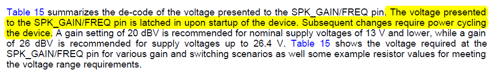
GVDD_REG power supply specification is not described in datasheet.
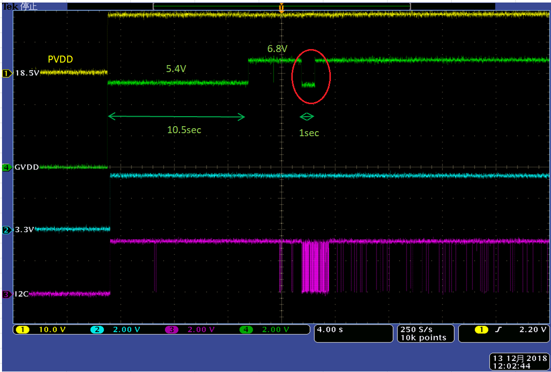
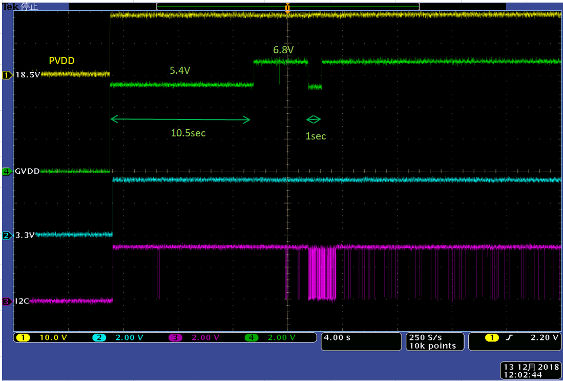
Waveform for startup sequence is attached below;
・On startup to 10 sec: 5.4V output and the after is 6.8V output.
・After I2C communication(Reset), GVDD is dropped to 5.4V for 1 sec and after become 6.8V.
Please let me know about two points question below;
①Is above waveform correct operation?
②Please let me know timing for read Vspk_GAIN/FREQ's DC voltage.
Best regards,
Satoshi