This thread has been locked.

If you have a related question, please click the "Ask a related question" button in the top right corner. The newly created question will be automatically linked to this question.

PCM5242: No output in hardware mode

Part Number: PCM5242

Hello,

As a learning exercise I am designing an audio DAC. I'm doing this in a modular way so as to be able to iterate on various stages, so each stage has headers for connecting to the next board. I've designed the first stage around the CP2615 which seems to work correctly. Now I am working on the DAC (I2S -> Analog), designed around the PCM5242 chip. This stage will output to the final stage, which will be the amplification stage.

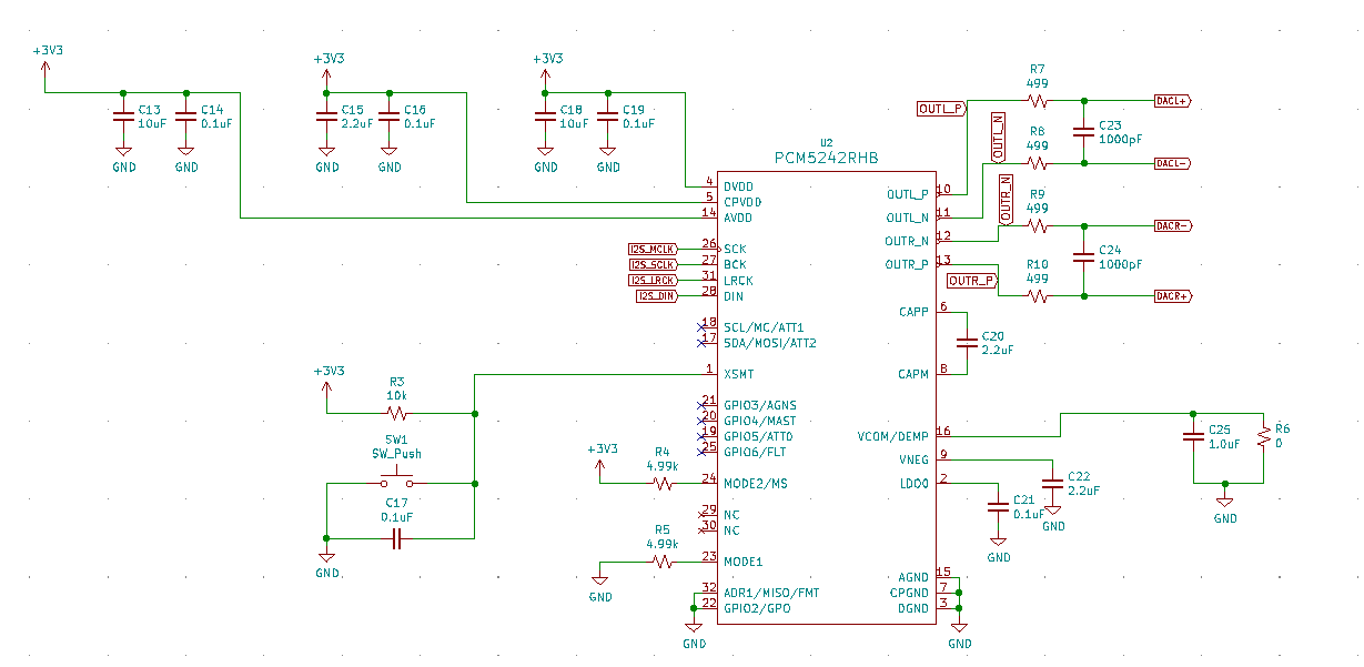
The relevant schematic portion is here, with some minor modifications (see below):

Notes/Changes:

  • R4 is not populated, MODE2 is jumpered to ground so as to set HARDWARE mode
  • R6 is not populated
  • I2S input signals @ 3.3V
  • CAPP/CAPM appear to be working correctly
  • VNEG is correctly creating -3.3V
  • LDO0 is correctly creating 1.8V
  • Input data format is 24-bit I2S

The issue: none of the output pins are showing any signal, and I'm not sure what to do to debug this. I've checked with a microscope that all of the connections look good -- what else might I try, or did I make a mistake on my schematic that might be causing this not to work as expected?

Thank you,

Jonathan

  • Hi Jonathan,

    If you have VNEG at ~-3.3V, then that means the clocks are supported, but I think it would still be good to verify your I2S format.
    What is the frequency of MCLK, BCK, and LRCK? Can you confirm that your host is actually providing data on the DIN line?

    Thanks,
    Paul
  • Any updates?
  • Unfortunately I’ve been away from this for a couple days but I will check tomorrow morning! When I looked at it last it *appeared* correct but I will take a closer look to be sure.

  • Ok, I've taken a look, and here's some traces:

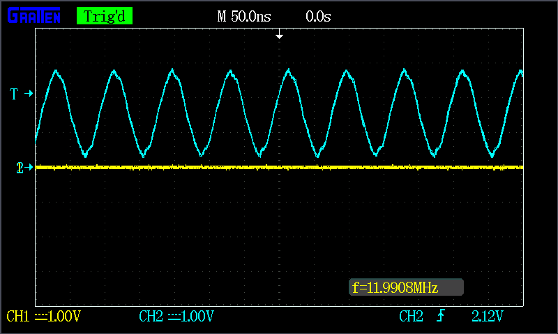
    MCLK @ 12MHz (Looks like it is a valid clock according to the datasheet):

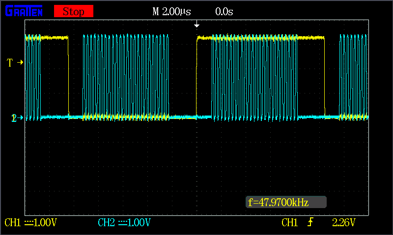
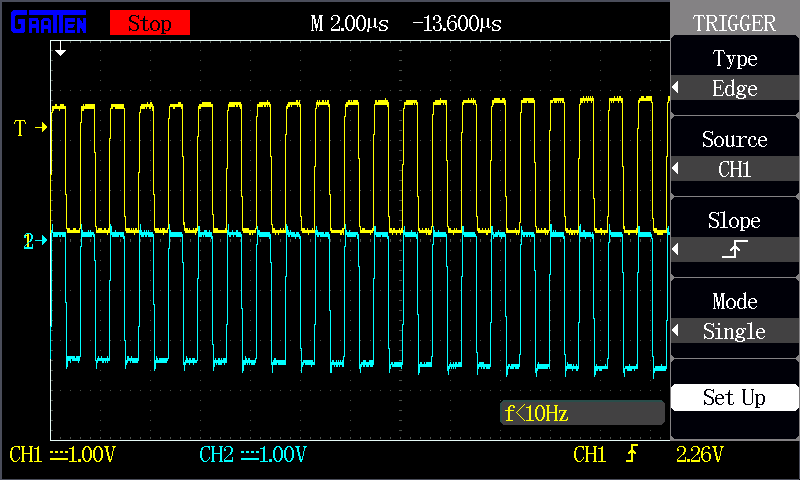
    SCLK & LRCLK (note: 24 SCLK per LRCLK, as expected for 24-bit I2S):

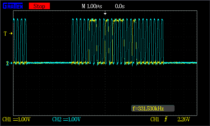
    SCLK & DIN:

    And just for good measure CAPP/CAPM:

    And yet still no output on either of the differential outputs? What else should I check?

    Thank you,

    Jonathan

  • Also probably worth mentioning: the outputs (DACL+/- and DACR+/-) are floating currently.
  • Hi Jonathan,

    I believe I understand the issue now.

    You have selected a I2S master that does not match the SCK requirements of the PCM5242 in hardware mode.  In hardware mode, using 4 wire I2S communication, you must have an SCK that matches table 32.  

    You may notice that all of these are 2^n multiples of the sample clock.  12MHz is not a 2^n multiple of 48k.  In the CP2615 PDS, they state that the master clock is 250×48kHz = 12MHz.  So the PCM5242 is having clock errors, as the LRCK is out of sync with SCK. 

    Now, normally you could just ground the SCK pin on the PCM5242 and use the device in 3-wire mode, but that will not work either.  The CP2615 has a higher frequency BCK than the required 64×48kHz BCK.  To overcome this, the BCK is not continuous.  Instead, it just pulses 32 bits at a time and then stops.  You can see this in your screen shots.  This is not a problem in 4-wire mode, but it makes BCK an invalid source clock for the PLL to generate the higher clock frequencies.  

    So you can either find another clock source for the CP2615, or use the device in software mode and source the 12MHz clock into one of the GPIO pins.  We describe this in the PDS:

    In this mode the PLL uses a GPIO as an input and another as an output, which is then connected to SCK.  You will need to use SPI/I2C to configure the PLL in that case.

    Let me know if you have questions on how to do that.

    Thanks,

    Paul


  • Hello,

    Thank you for this -- that does indeed appear to be the issue. I had seen that table (and Section 8.8.2) but wasn't really sure how to interpret it. My line of thought was that 12.288MHz (48kHz * 256) was within the +/4% tolerance at 12MHz, but apparently this was an incorrect interpretation.

    I'll re-evaluate some design choices to see if I want to add an MCU or something to configure the PCM524 and/or CP2615. Currently I designed the PCB without bringing out any of the pins for software mode.

    Thank you!
    Jonathan