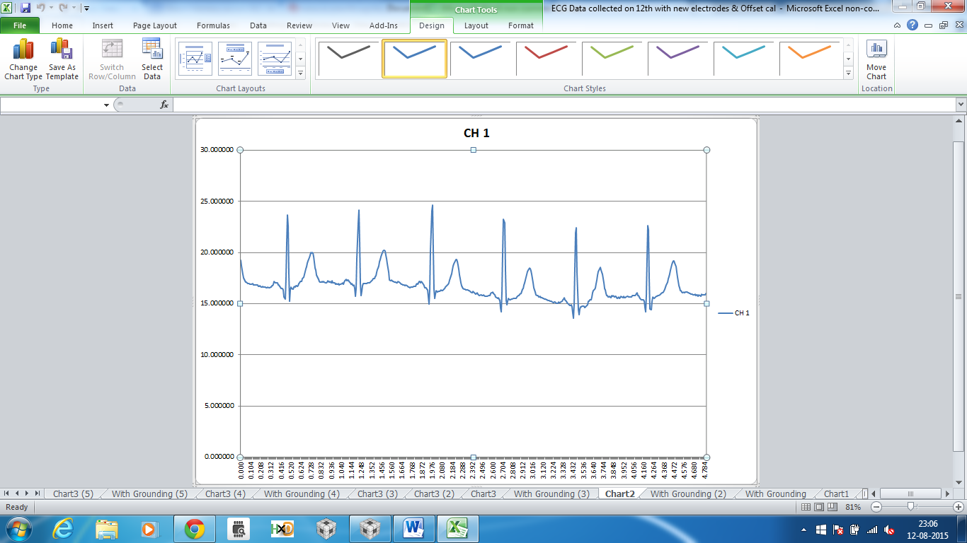
This thread has been locked.

If you have a related question, please click the "Ask a related question" button in the top right corner. The newly created question will be automatically linked to this question.

reading registers of ADS1292 return 0x00

Other Parts Discussed in Thread: MSP430F5529, ADS1292, ADS1292R

Hi,

I am using the sample code from the ADS1292 EVM in a CDC send data in background example of MSP430F5529 LP. The ACLK is chosen to be the XT2 crystal (4 MHz on the launch pad), the bit div is set to 4:

UCS0BR0 = 4

UCB0BR1 = 0

this should give a frequency of the SCLK as 1 MHz

When the registers are being read the ID register is returning a value of 0x00 while it should be 0x53. All the other registered are written but when read back are returning 0x00. I am unable to find the problem.

The example chose the ACLK source to be the REFO = 32kHz

after the setting I have inserted the following code


P5SEL |= 0x0C;
UCSCTL4 = (UCSCTL4 & ~(SELA_7)) | (SELA__XT2CLK);

This should change the ACLK source to XT2

Please suggest the solution.

Regards

Viney Chaddha

  • Brian,

    In fact you were right about the latency issue, I was trying to write different sectors with raw and processed data in a while loop and that was probably taking a long time. I removed the writing of the processed data, reduced the sampling rate and also increased the clock frequency from 8 MHz to 24 MHz and now I am able to get a clean ECG. Given below is the screen shot.

    Now I have a few more questions:

    1.) When I try to capture data with the laptop in the charging mode I get a lot of noise in the received data, should the RLD not take of that? If yes I am not sure if the RLD is correctly configured or not. My register settings are given below:


    //Device ID read Ony
    0x00,
    //CONFIG1 (default is 0x02 500 SPS)
    0x00,
    //CONFIG2 (default is 0xA0)
    0xA0,
    //LOFF
    0xF0,
    //CH1SET (PGA gain = 6)(default is 0x00)
    0x00,
    //CH2SET (PGA gain = 6)(default is 0x00)
    0x00,
    //RLD_SENS (default)(defalut is 0x2c)
    0x2C,
    //LOFF_SENS (default)
    0x0F,
    //LOFF_STAT
    0x00,
    //RESP1
    0x02,

    //RESP2
    0x13,
    //GPIO
    0x0C
    };

    Is the configuration correct for the RLD, How do I know if the RLD is functioning or not?

    2. Different time I have seen the ECG has large off sets - CH 1 output is sometime +ve and some time the output starts with a F- a negetive number as per the two2 complement, hence I gave the OPcode OFFSETCAL after wring the registers and a delay of 300 mS for the ADS1292 to settle down. but I still see that variation in the offsets in the readings. What factors other than the OPCODE can be responsible for it as on a human body the potential is +between RA and LA and RA and LL when the RA is connected to the INnN. so if the offset is cancelled one should see a positive value.

    3. I need to understand the maths behing the sample code that came with the EVM

    {
    			   ADS1x9x_ECG_Data_buf[1] = ADS1x9x_ECG_Data_buf[1] >> 4;
    			   ADS1x9x_ECG_Data_buf[2] = ADS1x9x_ECG_Data_buf[2] >> 4;
    	
    			   ADS1x9x_ECG_Data_buf[1] &= 0xFFFF;
    			   ADS1x9x_ECG_Data_buf[2] &= 0xFFFF;
    			   
    			   ECGRawData[0] = (short)ADS1x9x_ECG_Data_buf[1];
    			   ECGRawData[1] = (short)ADS1x9x_ECG_Data_buf[2];
    			   ECG_ProcessCurrSample_ch0(&ECGRawData[0],&ECGFilteredData[0]);
    			   ECG_ProcessCurrSample(&ECGRawData[1],&ECGFilteredData[1]);
    			   QRS_Algorithm_Interface(ECGFilteredData[1]);
    				
    			}
    
    void ECG_ProcessCurrSample_ch0(short *CurrAqsSample, short *FilteredOut)
    {
    
     	static unsigned short ECG_ch0_bufStart=0, ECG_ch0_bufCur = FILTERORDER-1, ECG_ch0FirstFlag = 1;
     	static short ECG_ch0_Pvev_DC_Sample, ECG_ch0_Pvev_Sample;
     	static short ECG_ch0_WorkingBuff[2 * FILTERORDER];
     	short *CoeffBuf;
     	
     	short temp1_ch0, temp2_ch0, ECGData_ch0;
     	
    
    	/* Count variable*/
    	unsigned short Cur_Chan_ch0;
    	short FiltOut_ch0;
    
    	CoeffBuf = CoeffBuf_40Hz_LowPass;					// Default filter option is 40Hz LowPass
    	if ( Filter_Option == 2)
    	{
    		CoeffBuf = CoeffBuf_50Hz_Notch;					// filter option is 50Hz Notch & 0.5-150 Hz Band
    	}
    	else if ( Filter_Option == 3)
    	{
    		CoeffBuf = CoeffBuf_60Hz_Notch;					// filter option is 60Hz Notch & 0.5-150 Hz Band
    	}
    	if  ( ECG_ch0FirstFlag )							// First time initialize static variables
    	{
    		for ( Cur_Chan_ch0 =0 ; Cur_Chan_ch0 < FILTERORDER; Cur_Chan_ch0++)
    		{
    			ECG_ch0_WorkingBuff[Cur_Chan_ch0] = 0;
    		} 
    		ECG_ch0_Pvev_DC_Sample = 0;
    		ECG_ch0_Pvev_Sample = 0;
    		ECG_ch0FirstFlag = 0;
    	}
    	temp1_ch0 = NRCOEFF * ECG_ch0_Pvev_DC_Sample;			// First order IIR
    	ECG_ch0_Pvev_DC_Sample = (CurrAqsSample[0]  - ECG_ch0_Pvev_Sample) + temp1_ch0;
    	ECG_ch0_Pvev_Sample = CurrAqsSample[0];
    	temp2_ch0 = ECG_ch0_Pvev_DC_Sample >> 2;
    	ECGData_ch0 = (short) temp2_ch0;
    
    	/* Store the DC removed value in Working buffer in millivolts range*/
    	ECG_ch0_WorkingBuff[ECG_ch0_bufCur] = ECGData_ch0;
    	/* */
    	ECG_FilterProcess(&ECG_ch0_WorkingBuff[ECG_ch0_bufCur],CoeffBuf,(short*)&FiltOut_ch0);
    	/* Store the DC removed value in ECG_WorkingBuff buffer in millivolts range*/
    	ECG_ch0_WorkingBuff[ECG_ch0_bufStart] = ECGData_ch0;
    
    	//FiltOut = ECGData[Cur_Chan];
    
    	/* Store the filtered out sample to the LeadInfo buffer*/
    	FilteredOut[0] = FiltOut_ch0 ;//(CurrOut);
    
    	ECG_ch0_bufCur++;
    	ECG_ch0_bufStart++;
    	if ( ECG_ch0_bufStart  == (FILTERORDER-1))
    	{
    		ECG_ch0_bufStart=0; 
    		ECG_ch0_bufCur = FILTERORDER-1;
    	}
    
    	return ;
    }

    The gain in the sample code is set to be 6

    the output is right shifted by 4, (number divided by 16) then 2 of the LSB bytes picked up ............some more processing and 

    it says the results are stored in the mV range. I have not really understood the maths behind this ALSO if the number is a 2's coplement  negetive number then one would loose the crucial sign of it as well? Could you please explain me the maths behind this.

    Regards

    Viney Chaddha

  • Hey Viney,

    Both issues are related to the RLD so I will address them together. To really take advantage of the capabilities of the RLD amplifier, set bit 4 of the RLD_SENS register. This will allow an average of the inputs specified by bits [3:0] of that register to serve as the input to the inverting RLD amplifier. The objective of inverting the input and outputting it on the body is to cancel shifts in the input voltages and cancel any noisy common mode signals. As far choosing which of those RLD_SENS[3:0] bits to set, I believe you have the RA electrode as the negative input to both channels so you need only set either bit 3 or 1 but not both. An example RLD_SENS register setting with the functionality I'm describing is 0x3D.

    The OFFSETCAL functionality will actually only account for offset introduced by the device itself so it will not remove the system level offset you are describing. Regarding the EVM source code, I did not write it as it was developed well before my time and to be honest, it confuses me at times. I can say, though, that it was created specifically for the EVM software so it is not optimized for an end application. In my opinion, I see the core usefulness in seeing the EVM source code for a customer being the ADC interface routines. The code for handling the data after it is collected is probably best developed by you.

    Regards,
    Brian Pisani
  • Brian,
    Whats the difference between bit(4 and Bit 5 of the RLD sense register, I thought the bit 4 i more for a lead off dtection, detailed explaination on these two bits would be of help

    In addition to that I I connect the shield to the ground  what effect do you anticipate? I can get you the actual plot tomorrow. Any clocking constraint for spi transfer, How fast can I go. Currently all SPI operations dene at 1mhz.

    Regards

    Viney Chaddha

  • Hey Viney,

    You're right; that bit is for RLD lead-off so it may be cleared. I'd still recommend including the channel 1 positive input as an input to the RLD amplifier. There are setup and hold constraints as well as period and duty-cycle requirements for the SPI interface, all of which may be found on page 10 of the datasheet.

    Brian Pisani
  • The OFFSETCAL functionality will actually only account for offset introduced by the device itself so it will not remove the system level offset you are describing

    Brian,

    Where do the random offsets in the system creep in, many times I see the offsets to be hugely negative and sometimes they are hugely positive, this is not limited to one channel, they happen randomly to any channel. What should be done to control them?
    Regards

    Viney Chaddha

  • Hey Viney,

    Have you included the positive input of channel 1 as a source of feedback to the RLD amplifier by setting bit 0 of the RLD_SENS register? If yes, how is the RL electrode connected to the patient simulator?

    Brian Pisani
  • Brian,
    The setting is 0x2C,
    Regards
    Viney Chaddha
  • Hey Viney,

    Try changing it to 0x2D.

    -Brian
  • What do you mean by negative DRDY edges at the output data rate?
    i am having the same problem, i just want to start the device and read one register.
  • Julia,
    What is the exact problem that you are facing? There have been a discussion on multiple issues in this thread. Let me know the exact nature of your problem and may be I am able to help you.
    Regards
    Viney Chaddha
  • Hello Viney

    I am using ADS1292R and i have connected it using arduino uno,
    I used the same circuit diagram as mention in the datasheet, and i have connected 4 wire SPI plus the RESET/PWDN, START, CLKSEL to GPIO in arduino. At first i want to read one register so i know that my communication is working,
    But all i am getting is zeros.


    Now before i send you my code here are some questions.

    1) is the circuit diagram that i used correct? or do i need any additional circuitry to start the device?
    2) MY device gets a bit hot as i start the SPI communication, is that ok?
    3) Can you please send me a simple code that can read the register with address 0x00?


    Here is the code that i am using


    #include <SPI.h>

    int ADS1292_DRDY_PIN = 6; /// Not used for now
    int ADS1292_CS_PIN = 10; ////// Working
    int ADS1292_START_PIN = 5; /// Working
    int ADS1292_PWDN_PIN = 4;////// Working
    int ADS1292_CLK_SEL = 3; /// Working


    int dat2 = 0;
    int dat1= 0;


    int RegData1 = 0;
    int RegData2 = 0;
    int RegData3 = 0;
    int RegData4 = 0;
    int RegData5 = 0;
    int RegData6 = 0;


    void setup() {
    pinMode(ADS1292_DRDY_PIN, INPUT); //6
    pinMode(ADS1292_CS_PIN, OUTPUT); //10
    pinMode(ADS1292_START_PIN, OUTPUT); //5
    pinMode(ADS1292_PWDN_PIN, OUTPUT); //4
    pinMode(ADS1292_CLK_SEL, OUTPUT); //3


    //////////// Power up sequence////////////
    delay(10);
    digitalWrite(ADS1292_PWDN_PIN, HIGH);
    delay(9000);
    digitalWrite(ADS1292_PWDN_PIN, LOW);
    delay(100);
    digitalWrite(ADS1292_PWDN_PIN, HIGH);
    delay(1000);
    ////////////////////////////////////////////


    ///// Set CLKSEL to 1////////////

    digitalWrite(ADS1292_CLK_SEL, LOW);
    delay(100);
    digitalWrite(ADS1292_CLK_SEL, HIGH);
    delay(10);
    //////////////////////////////////////////


    /////// Setting start pin to LOW////////
    digitalWrite(ADS1292_START_PIN, LOW);
    delay(100);

    SPI.begin();
    SPI.beginTransaction(SPISettings(1000000,MSBFIRST,SPI_MODE1));

    delay(1000); // Wait for SPI to begin

    Serial.begin(9600);


    }


    void loop() {
    // Sending the first command to ADS for SDAC so registers can be written

    digitalWrite(ADS1292_CS_PIN, LOW);
    delayMicroseconds(5);
    SPI.transfer(0b00000010); //// SPI Command for Wakeup
    delayMicroseconds(5);
    SPI.transfer(0b00010001); //// SPI Command to STOP read data continous mode
    delayMicroseconds(5);


    SPI.transfer(0b00100000); // Read register command
    delayMicroseconds(5);
    SPI.transfer(0b00000000); // Number of Registers to read
    delayMicroseconds(5);
    RegData1 = SPI.transfer(0b00000000);// Dummy Data
    delayMicroseconds(1);
    RegData2 = SPI.transfer(0b00000000);// Dummy Data
    delayMicroseconds(1);
    RegData3 = SPI.transfer(0b00000000);// Dummy Data
    delayMicroseconds(1);
    RegData4 = SPI.transfer(0b00000000);// Dummy Data
    delayMicroseconds(1);
    RegData5 = SPI.transfer(0b00000000);// Dummy Data
    delayMicroseconds(1);
    RegData6 = SPI.transfer(0b00000000);// Dummy Data
    delayMicroseconds(1);

    digitalWrite(ADS1292_CS_PIN, HIGH);


    Serial.print(RegData1,HEX);
    Serial.print("\t");
    Serial.print(RegData2,HEX);
    Serial.print("\t");
    Serial.print(RegData3,HEX);
    Serial.print("\t");
    Serial.print(RegData4,HEX);
    Serial.print("\t");
    Serial.print(RegData5,HEX);
    Serial.print("\t");
    Serial.print(RegData6,HEX);
    Serial.print("\n");


    }
  • Julia,
    The device should not be getting hot, check your connections and verify the device that you are using is good. You don't seem to be following the sequence as laid out in the ADS1292 datasheet page 63 and also check the SPI mode1 - the definition in TI is different so ensure that CPOL and CPHA settings are correct.
    Regards
    Viney Chaddha
  • as i told you that i am a beginner, would you kindly explain the sequence? or send me a code example so i can understand from that?
  • Can you please send me the code to read one register and print on serial monitor
  • Julian,
    I shall send you a psudocode tomorrow. Its late at night here in India and I am going to hit the bed soon. Sorry to keep you waiting.
    Regards
    Viney Chaddha
  • Thanks alot,
    and also let me know the status of the "START, PWDN/RESET,DRDY,CLKSEL" pins, what should be the level of these pins? High or low
    I will be waiting for your response.
  • Julia,
    For the internal clock set pins in following sequence:

    CLKSEL pin = high
    PWDN/RESET pin = high
    wait for 1 sec to reset
    CS pin = low
    PWDN/RESET = low
    wait 1 mS
    PWDN/REST = High
    START = low
    wait 1 mS
    START = High
    wait 5 mS
    CS = high
    wait 1 mS
    CS = low
    wait 1 mS
    Issue RDATAC command
    CS = High
    Enable interrupt for DRDY
    START = High

    This sequence has worked for me. May be he delays are more than required. Try and see.
    Regards
    Viney Chaddha
  • Hello Viney
    Thanks for this update, i tried this sequence, but i am still having problems with reading the register,
    i am not able to understand the procedure,
    kindly send me a psudocode to read a register and print it.
  • Julia,
    Share your mail Id I will mail it to you.
    Regards
    Viney Chaddha
  • juliasus92@gmail.com