This thread has been locked.

If you have a related question, please click the "Ask a related question" button in the top right corner. The newly created question will be automatically linked to this question.

ADS1259 ANALOG FORT END FOR +/-1000 VOLT AND +/-10 AMP DC CURRENT MEASUREMENT HELP AND SUGGESTION

Other Parts Discussed in Thread: OPA376, ADS1256, ADS1259, LM317, LM337, TINA-TI

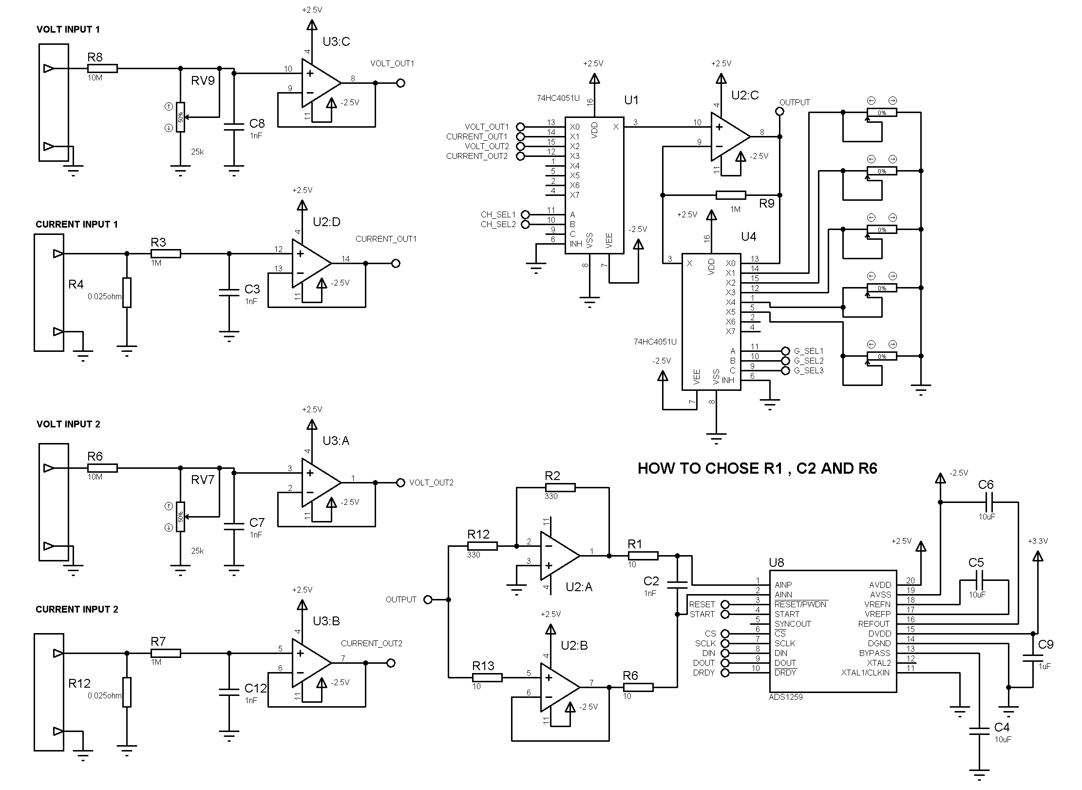
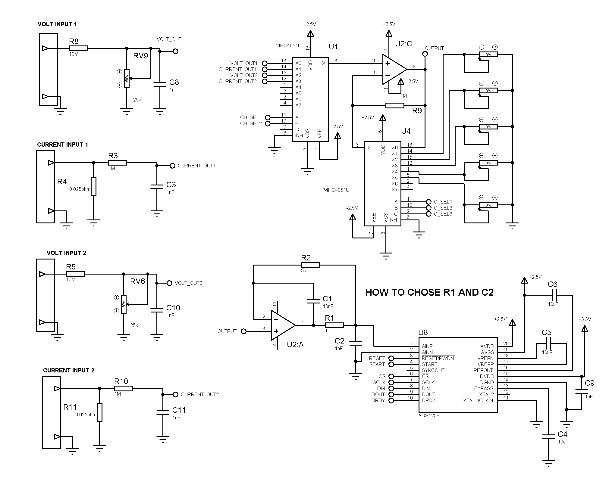
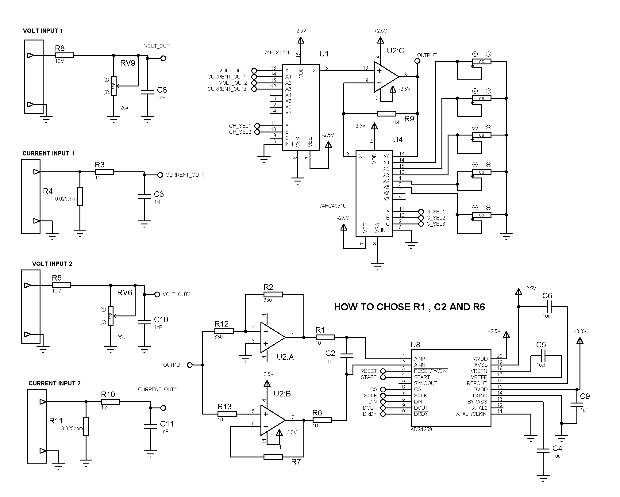
I am trying build high precision analog front end with pga option i searched almost mostly of pga amplifier but i was not able to find a suitable ic for my project it took allot of time to get at this point and so far i am looking for TI specialist  help to improvement / correction  in my attached circuit diagrams for ads1259b input stage and analog signal input stage specially resistance and capacitor calculation for ads1259b input stage 

these are goals which i want to achieve with this circuit

measure voltage in microvolt range using ads1259b

where my voltage input can be from 0 to +/-1000 volt dc

measure current from 0 to +/- 10 ampere dc in micro ampere range 

get maximum noise free bits resolution from ads1259b

for ac current and ac volt measurement i want that in buffer section input resistors and capacitor for ads1259b have optimized values for high data sampling rate 

all opamp are opa376 low noise opamp with low offset drift 

i draw almost four different configuration circuit to get feed back that which will work better and which have what kind of draw backs

here two diagrams with single ended input to ads1259b

here i have question that what if i dont use buffer before 74hc4051 ic which is same way as many other multichannel adc use like ads1256 have analog multiplexer before buffer amplifier this approach simplifies my circuit diagram as well reduce manufacture cost 

second question is as i am using dual supply and internal reference is bypassed with 10uF capicotor  grounded with -2.5 volt rail is this correct configuration i had checked ads1259 evm diagram and it appears in this way in that circuit 

third question is what would be full scale input voltage when ads1259b is driven by single ended input and what would be in case of fully differential input stage so based on this scale i can attenuate input volt using voltage divider

as i am using dual supply so i dont think that there would be any benifitt to drive adc with fully deffrential way where if i am correct according to data sheet then it is equal to +- Vref and internal vref is 2.5 volt so full scale should be +2.5 volt to -2.5 volt which dual supply single opamp circuit can drive  to ads1259b input 

what maximum noise free resolution is achievable circuits shown here with 2 layer pcb where botom layer is only ground plane and pcb is well designed separate analog and digital ground plane 

where case no1 driven by dc battery power source like to nimh cells in series ( 2.4 volt per 2 cells) for positive and negative rail where battery low volt range will be +/-2 volts does this will work on +-2 volts supply and avss to avdd total 4 volts and what kind of performance loss is expected on these working volts rather than standred working volt

case no2 driven by dual dc battery with lm317 / lm337 regulator for +- 2.5 volt 

case no3 driven by low noise linear regulator so power supply noise will not effect the adc resolution 

and  sorry to ask too many question in one time but i want that in reply of this post i would start working on pcb designing 

second with individual buffer before pga

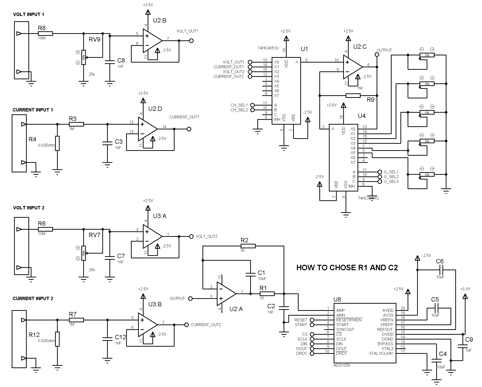
these two are with differential driver to ads1295 input 

and with individual buffer before multiplexer 

  • Hi Shams,

    See my responses to each question below:

    1) what if i dont use buffer before 74hc4051 ic which is same way as many other multichannel adc use like ads1256 have analog multiplexer before buffer amplifier this approach simplifies my circuit diagram as well reduce manufacture cost 

    The leakage current of the 74HC4051 is “relatively high”.  The 0.1uA leakage current across the large input resistors will create significant errors. For example, 0.1uA through 25kOhms is 2.5mV. If you use buffers, then consider the input bias currents of each buffer.

    2) as i am using dual supply and internal reference is bypassed with 10uF capicotor  grounded with -2.5 volt rail is this correct configuration i had checked ads1259 evm diagram and it appears in this way in that circuit 

    That’s correct.

     3) what would be full scale input voltage when ads1259b is driven by single ended input and what would be in case of fully differential input stage so based on this scale i can attenuate input volt using voltage divider

    For bipolar supplies and with AINN tied to 0V, AINP can swing +/-2.5V. You will not lose input dynamic range if you bias/level shift the ADC input buffer stage to provide the negative input swing.

     4) what maximum noise free resolution is achievable circuits shown here with 2 layer pcb where botom layer is only ground plane and pcb is well designed separate analog and digital ground plane

    The noise performance is a function of many variables. If you start with a good layout you can get close to the ADC’s noise performance. Then adding amplifiers and other components to the input will add to the noise. You can estimate the amplifier’s noise contribution if you know the noise density and the effective bandwidth. For exampling, if the noise density is 50nV/sqrt(Hz) (ignoring 1/f noise) and the effective bandwidth of your amplifier/filter is 10kHz, the noise contribution is 50nV * sqrt(10,000) = 5 uVrms.

     5) where case no1 driven by dc battery power source like to nimh cells in series ( 2.4 volt per 2 cells) for positive and negative rail where battery low volt range will be +/-2 volts does this will work on +-2 volts supply and avss to avdd total 4 volts and what kind of performance loss is expected on these working volts rather than standred working volt

    Below a supply voltage of 4.75V you’ll see performance degradation. I don’t have data to tell me how much performance degradation you might see.

     6) How to choose R1 and C2

    I recommend simulating this in TINA-TI. You’ll have to come up with a trade-off in performance. Larger time constants will make for a better filter, but you’ll see increased settling time and op amp stability issues (especially as C gets larger). Usually R1 is in the range of 20-200 Ohms and C2 is in the range of 100pF to 1nF.


    Best Regards,
    Chris